Register once, drag and drop ECAD models into your CAD tool and speed up your design.
Click here for more information74AVCH2T45GD
Dual-bit, dual-supply voltage level translator/transceiver; 3-state
The 74AVCH2T45 is a dual bit, dual supply transceiver that enables bidirectional level translation. It features two data input-output ports (nA and nB), a direction control input (DIR) and dual supply pins (VCC(A) and VCC(B)). Both VCC(A) and VCC(B) can be supplied at any voltage between 0.8 V and 3.6 V making the device suitable for translating between any of the low voltage nodes (0.8 V, 1.2 V, 1.5 V, 1.8 V, 2.5 V and 3.3 V). Pins nA and DIR are referenced to VCC(A) and pins nB are referenced to VCC(B). A HIGH on DIR allows transmission from nA to nB and a LOW on DIR allows transmission from nB to nA.
The device is fully specified for partial power-down applications using IOFF. The IOFF circuitry disables the output, preventing any damaging backflow current through the device when it is powered down. In suspend mode when either VCC(A) or VCC(B) are at GND level, both A and B are in the high-impedance OFF-state.
The 74AVCH2T45 has active bus hold circuitry which is provided to hold unused or floating data inputs at a valid logic level. This feature eliminates the need for external pull-up or pull-down resistors.
Alternatives
Features and benefits
Wide supply voltage range: 0.8 V to 3.6 V for VCC(A) and VCC(B)
High noise immunity
Suspend mode
Bus hold on data inputs
Inputs accept voltages up to 3.6 V
Low noise overshoot and undershoot < 10 % of VCC
IOFF circuitry provides partial Power-down mode operation
Maximum data rates:
500 Mbps (1.8 V to 3.3 V translation)
320 Mbps (< 1.8 V to 3.3 V translation)
320 Mbps (translate to 2.5 V or 1.8 V)
280 Mbps (translate to 1.5 V)
240 Mbps (translate to 1.2 V)
Latch-up performance exceeds 100 mA per JESD 78 Class II
Complies with JEDEC standards:
JESD8-12 (0.8 V to 1.3 V)
JESD8-11 (0.9 V to 1.65 V)
JESD8-7 (1.2 V to 1.95 V)
JESD8-5 (1.8 V to 2.7 V)
JESD8-B (2.7 V to 3.6 V)
ESD protection:
HBM: ANSI/ESDA/Jedec JS-001 Class 3B exceeds 8000 V
CDM: ANSI/ESDA/Jedec JS-002 Class C3 exceeds 1000 V
Multiple package options
Specified from -40 °C to +85 °C and -40 °C to +125 °C
Parametrics
| Type number | Product status | Package name |
|---|---|---|
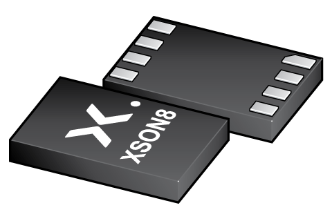
| 74AVCH2T45GD | End of life | XSON8 |
Package
All type numbers in the table below are discontinued.
| Type number | Orderable part number, (Ordering code (12NC)) | Status | Marking | Package | Package information | Reflow-/Wave soldering | Packing |
|---|---|---|---|---|---|---|---|
| 74AVCH2T45GD | 74AVCH2T45GD,125 (935288283125) |
Obsolete | K45 |
XSON8 (SOT996-2) |
SOT996-2 | SOT996-2_125 |
Environmental information
All type numbers in the table below are discontinued.
| Type number | Orderable part number | Chemical content | RoHS | RHF-indicator |
|---|---|---|---|---|
| 74AVCH2T45GD | 74AVCH2T45GD,125 | 74AVCH2T45GD |
|
|
Series
Documentation (7)
| File name | Title | Type | Date |
|---|---|---|---|
| 74AVCH2T45 | Dual-bit, dual-supply voltage level translator/transceiver; 3-state | Data sheet | 2022-12-07 |
| AN10161 | PicoGate Logic footprints | Application note | 2002-10-29 |
| AN90007 | Pin FMEA for AVC family | Application note | 2018-11-30 |
| Nexperia_document_guide_Logic_translators | Nexperia Logic Translators | Brochure | 2021-04-12 |
| avch2t45 | 74AVCH2T45 Ibis model | IBIS model | 2014-10-14 |
| Nexperia_package_poster | Nexperia package poster | Leaflet | 2020-05-15 |
| SOT996-2 | plastic, leadless extremely thin small outline package; 8 terminals; 0.5 mm pitch; 3 mm x 2 mm x 0.5 mm body | Package information | 2020-04-21 |
Support
If you are in need of design/technical support, let us know and fill in the answer form we'll get back to you shortly.
Models
| File name | Title | Type | Date |
|---|---|---|---|
| avch2t45 | 74AVCH2T45 Ibis model | IBIS model | 2014-10-14 |
How does it work?
The interactive datasheets are based on the Nexperia MOSFET precision electrothermal models. With our interactive datasheets you can simply specify your own conditions interactively. Start by changing the values of the conditions. You can do this by using the sliders in the condition fields. By dragging the sliders you will see how the MOSFET will perform at the new conditions set.
74AVCH2T45GD
Dual-bit, dual-supply voltage level translator/transceiver; 3-state
Buy from Nexperia
| SKU | Stock* | MOQ | Price per unit | Quantity |
|---|
Buy from distributors
| Seller | SKU | Stock | MOQ | 1 | 10 | 100 | 1,000 | 10,000 | Purchase |
|---|
| Seller | SKU | Stock | MOQ | 1 | 10 | 100 | 1,000 | 10,000 | Purchase |
|---|
| Seller | SKU | Stock | MOQ | 1 | 10 | 100 | 1,000 | 10,000 | Purchase |
|---|
| Seller | SKU | Stock | MOQ | 1 | 10 | 100 | 1,000 | 10,000 | Purchase |
|---|
| Seller | SKU | Stock | MOQ | 1 | 10 | 100 | 1,000 | 10,000 | Purchase |
|---|
** Displayed price per unit is based on small quantity orders
*** Authorized resellers for overstock, mature, and discontinued products which are warranted for reliability by the reseller, no longer by Nexperia>