
Register once, drag and drop ECAD models into your CAD tool and speed up your design.
Click here for more information74LVC1T45GF
Dual supply translating transceiver; 3-state
The 74LVC1T45; 74LVCH1T45 are single bit, dual supply transceivers with 3-state outputs that enable bidirectional level translation. They feature two 1-bit input-output ports (A and B), a direction control input (DIR) and dual supply pins (VCC(A) and VCC(B)). Both VCC(A) and VCC(B) can be supplied at any voltage between 1.2 V and 5.5 V making the device suitable for translating between any of the low voltage nodes (1.2 V, 1.5 V, 1.8 V, 2.5 V, 3.3 V and 5.0 V). Pins A and DIR are referenced to VCC(A) and pin B is referenced to VCC(B). A HIGH on DIR allows transmission from A to B and a LOW on DIR allows transmission from B to A.
The devices are fully specified for partial power-down applications using IOFF. The IOFF circuitry disables the output, preventing any damaging backflow current through the device when it is powered down. In suspend mode when either VCC(A) or VCC(B) are at GND level, both A port and B port are in the high-impedance OFF-state.
Active bus hold circuitry in the 74LVCH1T45 holds unused or floating data inputs at a valid logic level.
Alternatives
Features and benefits
Wide supply voltage range:
VCC(A): 1.2 V to 5.5 V
VCC(B): 1.2 V to 5.5 V
High noise immunity
Maximum data rates:
420 Mbps (3.3 V to 5.0 V translation)
210 Mbps (translate to 3.3 V))
140 Mbps (translate to 2.5 V)
75 Mbps (translate to 1.8 V)
60 Mbps (translate to 1.5 V)
Suspend mode
Latch-up performance exceeds 100 mA per JESD 78 Class II
±24 mA output drive (VCC = 3.0 V)
Inputs accept voltages up to 5.5 V
Low power consumption: 16 μA maximum ICC
IOFF circuitry provides partial Power-down mode operation
Complies with JEDEC standards:
JESD8-7 (1.2 V to 1.95 V)
JESD8-5 (1.8 V to 2.7 V)
JESD8C (2.7 V to 3.6 V)
JESD36 (4.5 V to 5.5 V)
ESD protection:
HBM: ANSI/ESDA/JEDEC JS-001 class 3A exceeds 4000 V
CDM: ANSI/ESDA/JEDEC JS-002 class C3 exceeds 1000 V
Multiple package options
Specified from -40 °C to +85 °C and -40 °C to +125 °C
Parametrics
| Type number | Product status | Package name |
|---|---|---|
|
74LVC1T45GF
|
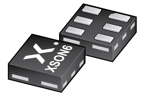
Not for design in | XSON6 |
PCB Symbol, Footprint and 3D Model
| Model Name | Description |
|---|---|
|
|
Series
Documentation (5)
| File name | Title | Type | Date |
|---|---|---|---|
| 74LVC_LVCH1T45 | Dual supply translating transceiver; 3-state | Data sheet | 2023-08-04 |
| AN10161 | PicoGate Logic footprints | Application note | 2002-10-29 |
| AN11009 | Pin FMEA for LVC family | Application note | 2019-01-09 |
| Nexperia_document_guide_Logic_translators | Nexperia Logic Translators | Brochure | 2021-04-12 |
| lvc1t45 | lvc1t45 IBIS model | IBIS model | 2013-04-08 |
Support
If you are in need of design/technical support, let us know and fill in the answer form we'll get back to you shortly.
Models
| File name | Title | Type | Date |
|---|---|---|---|
| lvc1t45 | lvc1t45 IBIS model | IBIS model | 2013-04-08 |
PCB Symbol, Footprint and 3D Model
| Model Name | Description |
|---|---|
|
|
Ordering, pricing & availability
Sample
As a Nexperia customer you can order samples via our sales organization or directly via our Online Sample Store: https://extranet.nexperia.com.
Sample orders normally take 2-4 days for delivery.
If you do not have a direct account with Nexperia our network of global and regional distributors is available and equipped to support you with Nexperia samples.
How does it work?
The interactive datasheets are based on the Nexperia MOSFET precision electrothermal models. With our interactive datasheets you can simply specify your own conditions interactively. Start by changing the values of the conditions. You can do this by using the sliders in the condition fields. By dragging the sliders you will see how the MOSFET will perform at the new conditions set.
74LVC1T45GF
Dual supply translating transceiver; 3-state
Buy from Nexperia
| SKU | Stock* | MOQ | Price per unit | Quantity |
|---|
Buy from distributors
| Seller | SKU | Stock | MOQ | 1 | 10 | 100 | 1,000 | 10,000 | Purchase |
|---|
| Seller | SKU | Stock | MOQ | 1 | 10 | 100 | 1,000 | 10,000 | Purchase |
|---|
| Seller | SKU | Stock | MOQ | 1 | 10 | 100 | 1,000 | 10,000 | Purchase |
|---|
| Seller | SKU | Stock | MOQ | 1 | 10 | 100 | 1,000 | 10,000 | Purchase |
|---|
| Seller | SKU | Stock | MOQ | 1 | 10 | 100 | 1,000 | 10,000 | Purchase |
|---|
** Displayed price per unit is based on small quantity orders
*** Authorized resellers for overstock, mature, and discontinued products which are warranted for reliability by the reseller, no longer by Nexperia>