Authors: Phil Ellis, Andrew Thomson & Reza Behtash; Application Engineers, Manchester & Hamburg.
This interactive application note contains embedded Cloud based simulations to augment the text.
To open the embedded simulation, simply hover over the simulation image. Left click anywhere in the graphic area once the central play button changes in colour. This opens the schematic in the Cloud environment. See the interactive application note tutorial page for more details on how to use the simulations. See accompanying application note AN50001.
1. Introduction
This aim of this interactive application note is to help the reader gain an insight into how to protect 12 V automotive systems from being exposed to a reversed biased battery condition e.g. during maintenance where the battery leads may be reconnected in the opposite polarity.
Four methods of reverse battery protection (RBP) are discussed:
- Recovery rectifier (PN diode)
- Schottky rectifier
- P-channel MOSFET
- N-channel MOSFET
The dominant losses in RBP applications are due to conduction. The ordering of the components in the above list is important as it gives an indication of the least capable to most capable methods. In other words for a particular current flow Recovery rectifiers exhibit the greatest loss and N-channel MOSFETs the least loss. Table 1 summarises the key factors of each method.
Recovery rectifier (PN diode)e.g. PNE20030EP in CPF5 |
 |
|
Schottky rectifiere.g. PMEG045T150EPD in CFP15 |
 |
|
P-channel MOSFETe.g. BUK6Y14-40P in LFPAK56E |
 |
|
N-channel MOSFETe.g. BUK7J1R4-40H in LFPAK56E |
 |
|

2. Recovery rectifier (PN diode) steady state conduction loss
Using a Recovery rectifier as a blocking diode can be considered as the simplest and most cost effective way to realize a reverse battery protection (RBP) circuit. Inserting a Recovery rectifier in series with the load ensures that current can flow only when the battery is correctly connected. There is no control input needed, resulting in a low complexity and low component count. The usage of a Recovery rectifier for RBP is however compromised by the high forward voltage drop of the PN junction. This is the reason why Recovery rectifiers are only used for low power applications (load currents below ~1 A).
Inrush current through the rectifier must be considered e.g. when the battery is switched into circuit and the bulk capacitance begins to charge. The peak current and duration of the pulse must be checked to ensure it does not exceed specification.
The steady state conduction losses, Ploss, can be calculated by using the forward voltage drop VF of the diode given for a steady state temperature of the PN junction and the load current Iload:
(Eq 1) 
The forward voltage drop of a PN junction decreases by -1.9 mV/K as the device heats up, lowering the losses at higher junction temperatures. Nevertheless the maximum total power dissipation of the Recovery rectifier has to be respected as indicated in the data sheet of the particular diode.
In the option examples above the PNE20030EP Recovery rectifier is identified as being well suited to this type of application. Using close to the example current in a simulation gives an indication of the expected forward voltage drop, junction and PCB temperatures, with the ambient temperature (on the product’s case) of 105 °C.
Click below to start the Recovery rectifier PNE20030EP simulation:
Simulation 1. Recovery rectifier PNE20030EP

3. Schottky rectifier steady state conduction loss
In order to overcome the high conduction losses of a Recovery rectifier, designers could use a Schottky rectifier for RBP. A Schottky device as blocking diode comes with the same advantages as a Recovery rectifier (least complexity). Thanks to its lower forward voltage drop it can be used for higher load currents up to approximately 3 A. However a Schottky rectifier comes with a higher leakage current due to its metal-semiconductor interface. The leakage current of a Schottky rectifier becomes significantly larger at higher junction temperatures, resulting in unwanted effects such as thermal runaway.
Similarly to the Recovery rectifier, inrush current through the diode must be considered e.g. when the battery is switched into circuit and the bulk capacitance begins to charge. The peak current and duration of the pulse must be checked to ensure it does not exceed specifications.
As in the case of the Recovery rectifier the conduction losses can be calculated by multiplying the temperature-dependent voltage drop with the load current (Eq 1).
Also for Schottky rectifiers the junction temperature must not exceed the specified maximum junction temperature which is 175 °C for automotive types.
In the option examples above the Schottky rectifier PMEG045T150EPD is identified as being well suited to this type of application. Using close to the example current in simulation gives an indication of the expected forward voltage drop, power dissipation, junction and PCB temperatures for an ambient temperature of 105 °C on the product’s case.
Click below to start the Schottky rectifier PMEG045T150EPD simulation:
Simulation 2. Schottky rectifier

4. P-channel MOSFET solution steady state conduction loss
In RBP applications the MOSFET can be considered as operating in two modes: “DIODE” mode and “MOSFET” mode. During manufacture a parasitic PN junction diode is created within each MOSFET cell, the antiparallel “diode” on the die actually comprises many parallel diodes distributed uniformly across the whole active die area.
When the MOSFET is not enhanced i.e. the gate terminal does not have a sufficiently negative voltage below its source to exceed its minimum threshold to turn-on then, with the battery connected correctly, it behaves as a forward biased DIODE. The power loss in the device is the product of the forward diode voltage and current flowing through it. The forward diode voltage decreases with increase in temperature by -1.9 mV/K. Therefore as the die heats the power dissipation reduces for a given current.
Once the gate-source threshold is reached the MOSFET becomes enhanced and switches from “DIODE” to “MOSFET” mode. Current then flows in the drain-source channel. The power loss is then the product of the on-state resistance RDSon and square of the current flowing in the channel. To illustrate the effect of DIODE mode self-heating the simulation delays enhancement to MOSFET mode for ~35 s,
Click below to start the P-channel MOSFET BUK6Y14-40P simulation:
Simulation 3. P-channel MOSFET BUK6Y14-40P
The P-channel simulation is initially set up with a slightly higher load current to the Schottky rectifier simulation.
To observe the device behaving as a diode look at the first portion of the junction temperature plot where the junction rises significantly above case temperature. Later observe the difference in power dissipation when the MOSFET is enhanced and switches from “DIODE” to “MOSFET” mode. If we consider a battery voltage of 13.5 V and VSD = 0.7 V typical at 25 °C, (values taken from the BUK6Y14-40P data sheet), driving a load resistance of 2.35 Ω. The expected power dissipation would be somewhere around 0.7 V × (13.5 V/2.35 Ω) = 0 .7 V × 5.75 A = ~4.02 W.
It will be shown that the effects of temperature soon modify this expected result. This is true because products within vehicles soon rise above this notional outside air ambient of 25 °C and the impact on component behaviour must be considered.

Temperatures above 125 °C are not uncommon dependent on product location within the vehicle and the ambient air temperature. However the focus here is on a product operating with a case temperature representing it being mounted on or near the engine jacket where the coolant temperature is expected to be around 105 °C.
Therefore what we see in the simulation is rather more accurate in that it accounts for the impedance presented by the diode and the drop in diode forward voltage as the die temperature rises. The load current is seen reduced to ~5.5 A and diode dissipation to ~3.07 W.
The mounting base temperature is that of the component’s location on the PCB. In other words there will be some mounting base offset temperature expected dependent on how good the thermal linkage is between the component’s mounting base (Tmb) and local pedestals connecting the component to the product’s external case (local ambient) temperature of 105 °C.
The steady state condition considers the PCB thermal resistance Rth value dominant rather than the transient Zth value. Simulation uses a Rth(PCB) of 30 K/W and reduced thermal capacitance to allow this dominance. If the device were left in DIODE mode the simulation shows the notional temperature on the PCB would be very close to the maximum junction temperature specification of 175 °C and damage to the PCB surface may result even though a high temperature material may have been chosen for the application.
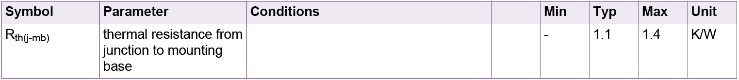
To illustrate the effect of DIODE mode self-heating the simulation delays enhancement to MOSFET mode for ~35 s. In this time, for a dissipation of 3.07 W, simulation shows Tmb has risen to 168.13 °C and Tj to 172.2 °C. We can make a calculation based on using the data sheet Rth(j-mb) maximum value of 1.4 K/W. For a power dissipation of 3.07 W we should expect the junction temperature to rise by 3.07 W × 1.4 K/W = 4.29 °C above Tmb.
This calculation yields a junction temperature of 172.42 °C which correlates reasonably well with the simulation indicating the model is using the same Rth(j-mb) max figure.
When the device has sufficient gate bias applied to enhance (turn-on) the MOSFET element the device behaves as having a resistance in parallel with the diode. The data sheet gives the typical and maximum values of the on-state resistance with a junction temperature of 25 °C.
The simulation results show that by 531 seconds after enhancement MOSFET power dissipation and Tmb have dropped significantly to near steady state values of 683.77 mW and 125.51 °C respectively. The load current has increased slightly to ~5.69 A indicating a reduction in line impedance presented by the MOSFET to the battery.
If we make a power loss calculation based on 5.69 A load current and RDSon, the formula changes from DIODE power = V × I to MOSFET power = I2R where I is drain current and R is RDSon, by substitution (5.6942) × 14 mΩ = 453.9 mW. So why is there such a discrepancy with the 683.78 mW shown in the simulation? The above calculation was made using RDSon maximum @ 25 °C neglecting to factor in temperature.
RDSon has a positive temperature coefficient, see Fig. 1. The simulation models how RDSon changes from that 14 mΩ maximum value at 25 °C to a 1.51 typical multiplier @ 125 °C. Using 1.51 × 14 mΩ = 21.14 mΩ we can expect a power dissipation of (5.6942) × 21.14 mΩ = 685.39 mW which correlates well with simulation.

Figure 1. BUK6Y14-40P normalized drain-source on-state resistance as a function of junction temperature; typical values
Now if the power dissipation is multiplied by Rth(j-mb) we see a junction temperature of 685.39 mW × 1.4 K/W = 0.956 °C above the mounting base temperature; 125.51 °C + 0.956 °C = 126.4695 °C which correlates very well with the junction temperature result of 126.47 °C seen in simulation.
As shown above simulation indicates the mounting base temperature will be around 125.51 °C with 5.694 A fowing through the device. There is a need to check the current derating for the BUK6Y14-40P when exposed to this elevated mounting base temperature.
The full rated continuous current is given in the data sheet as 64 A at 25°C.


The BUK6Y14-40P data sheet specifies the maximum permitted drain current at 25 °C and 100 °C.
The maximum drain current derating for temperature is given by the equation below, where maximum junction temperature Tj = 175 °C:
(Eq 2) 
Hence the maximum permissible drain current = √[(175-125.51)/(175-25)] = 0.57 of full rated value @ 25°C. This gives a value of 64 A * 0.57 = 36.8 A, so we have excellent margin.
If the threshold voltage falls to -1 V the device is guaranteed to be off, (see Fig. 2) and the DIODE will be the only conduction path.
Hence losses when the device is in DIODE mode are large compared to when the device is operating in MOSFET mode making the MOSFET ideally suited to larger current, high temperature RBP applications.

5. N-channel MOSFET solution steady state conduction loss
The majority of the description of P-channel behaviour also applies to N-channel devices. The major difference being that to enhance an N-channel device into MOSFET mode its gate must be biased positively with respect to its source.
Importantly the N-channel MOSFET is capable of conducting larger currents as the RDSon value for a particular die size is much lower than that of a P-channel device. The significantly lower power dissipation in MOSFET mode means that the N-channel device is much better suited for applications demanding larger currents.
The N-channel simulation uses as an example 24.5 A rather than 5.69 A of the P-channel simulation. This is based on an ambient temperature of 105 ˚C and a near stable Tj of 140 ˚C. The power dissipated in the MOSFET is around 1.165 W at 140 ˚C. The circuit board material used is assumed to be suitable for such high temperatures (“normal” FR4 is capable to around 105 ˚C only, this is the ambient temperature here).
Referring to the simulation it can be seen that the source is at the battery positive voltage. Therefore to bias the gate above battery positive voltage a charge pump is normally required. To prevent the MOSFET being in linear mode where its RDSon would cause the device to dissipate more power than desirable, gate switching must be delayed until a satisfactory threshold voltage can be achieved.
In the simulation, there is a 30 second delay before the MOSFET switches on. During this time, the full load current is passing through the MOSFET body diode and the junction temperature reaches a peak of 175 ˚C. The power dissipated in the device is around 15 W. This demonstrates that by switching on the MOSFET, a significant power saving can be achieved.
Click below to start the N-channel MOSFET BUK7J1R4-40H simulation:
Simulation 4. N-channel MOSFET
Summary
The four key methods of reverse battery protection have been discussed.
Guidance has been provided to clarify the best approach to meet demands of the application while achieving optimal cost and performance.
Nexperia offers products which are very well suited for RBP applications.
Choose from very cost-effective Recovery rectifiers or Schottky rectifiers as solutions for lower power applications. Choose from P-channel and N-channel MOSFETS as the load current increases. Nexperia offers a range of thermally and electrically efficient device packages to support each area of application. Interactive electrothermal simulations of the application have been embedded into this application note to assist in that selection process. Watch the demo video below.
PartQuest embedded Cloud simulations were used in this interactive application note.
Reverse battery protection solutions demo
Youtube video
| Page last updated 29 November 2021. |