
Features and benefits
-
Wide supply voltage range from 1.2 to 3.6 V
-
CMOS low power consumption
-
Direct interface with TTL levels
-
Overvoltage tolerant inputs to 5.5 V
-
High-impedance when VCC = 0 V
-
8-bit positive edge-triggered register
-
Independent register and 3-state buffer operation
-
Flow-through pin-out architecture
-
IOFF circuitry provides partial Power-down mode operation
-
Complies with JEDEC standard:
-
JESD8-7A (1.65 V to 1.95 V)
-
JESD8-5A (2.3 V to 2.7 V)
-
JESD8-C/JESD36 (2.7 V to 3.6 V)
-
-
ESD protection:
-
HBM: ANSI/ESDA/JEDEC JS-001 class 2 exceeds 2000 V
-
CDM: ANSI/ESDA/JEDEC JS-002 class C3 exceeds 1000 V
-
-
Specified from -40 °C to +85 °C and -40 °C to +125 °C
Parametrics
| Type number | Product status | VCC (V) | Logic switching levels | Output drive capability (mA) | tpd (ns) | fmax (MHz) | Power dissipation considerations | Tamb (°C) | Rth(j-a) (K/W) | Ψth(j-top) (K/W) | Rth(j-c) (K/W) | Package name |
|---|---|---|---|---|---|---|---|---|---|---|---|---|
| 74LVC574ABQ | Production | 1.2 - 3.6 | CMOS/LVTTL | ± 24 | 3.2 | 150 | low | -40~125 | 79 | 9.5 | 50 | DHVQFN20 |
| 74LVC574AD | Production | 1.2 - 3.6 | CMOS/LVTTL | ± 24 | 3.2 | 150 | low | -40~125 | 85 | 27.6 | 61 | SO20 |
| 74LVC574APW | Production | 1.2 - 3.6 | CMOS/LVTTL | ± 24 | 3.2 | 150 | low | -40~125 | 101 | 4.7 | 45 | TSSOP20 |
Package
| Type number | Package | Package information | Reflow-/Wave soldering | Packing | Status | Marking | Orderable part number, (Ordering code (12NC)) |
|---|---|---|---|---|---|---|---|
| 74LVC574ABQ | 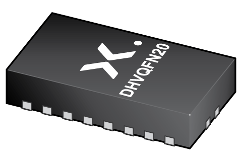 DHVQFN20 (SOT764-1) | SOT764-1 | SOT764-1_115 | Active | LVC574A | 74LVC574ABQ,115 ( 9352 735 17115 ) | |
| 74LVC574AD | 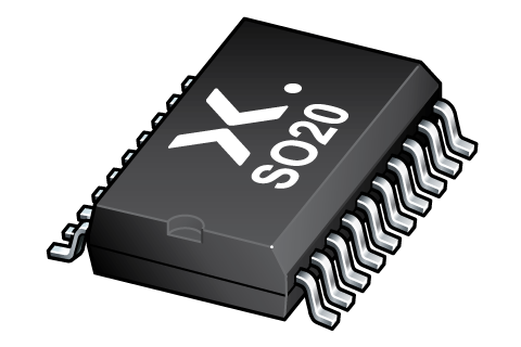 SO20 (SOT163-1) | SOT163-1 | WAVE_BG-BD-1 | SOT163-1_118 | Active | 74LVC574AD | 74LVC574AD,118 ( 9352 190 30118 ) |
| 74LVC574APW | 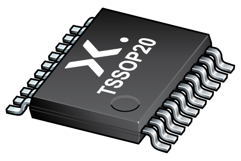 TSSOP20 (SOT360-1) | SOT360-1 | SSOP-TSSOP-VSO-WAVE | SOT360-1_118 | Active | LVC574A | 74LVC574APW,118 ( 9352 190 50118 ) |
The variants in the table below are discontinued. See the table Discontinuation information for more information.
| Type number | Package | Package information | Reflow-/Wave soldering | Packing | Status | Marking | Orderable part number, (Ordering code (12NC)) |
|---|---|---|---|---|---|---|---|
| 74LVC574AD | SO20 (SOT163-1) | SOT163-1 | WAVE_BG-BD-1 | SOT163-1_112 | Withdrawn / End-of-life | 74LVC574AD | 74LVC574AD,112 ( 9352 190 30112 ) |
| 74LVC574APW | TSSOP20 (SOT360-1) | SOT360-1 | SSOP-TSSOP-VSO-WAVE | SOT360-1_112 | Withdrawn / End-of-life | LVC574A | 74LVC574APW,112 ( 9352 190 50112 ) |
Discontinuation information
| Type number | Orderable part number, (Ordering code (12NC)) | Last time buy date | Last time delivery date | Replacement product | Status | Comments |
|---|---|---|---|---|---|---|
| 74LVC574AD | 935219030112 | 2021-12-31 | 2022-06-30 | 74LVC574AD | ||
| 74LVC574APW | 935219050112 | 2021-12-31 | 2022-06-30 | 74LVC574APW |
Environmental information
| Type number | Orderable part number | Chemical content | RoHS | RHF-indicator | Leadfree conversion date |
|---|---|---|---|---|---|
| 74LVC574ABQ | 74LVC574ABQ,115 | 74LVC574ABQ | Always Pb-free | ||
| 74LVC574AD | 74LVC574AD,118 | 74LVC574AD | week 30, 2004 | ||
| 74LVC574APW | 74LVC574APW,118 | 74LVC574APW | week 7, 2005 |
The variants in the table below are discontinued. See the table Discontinuation information for more information.
| Type number | Orderable part number | Chemical content | RoHS | RHF-indicator | Leadfree conversion date |
|---|---|---|---|---|---|
| 74LVC574AD | 74LVC574AD,112 | 74LVC574AD | week 30, 2004 | ||
| 74LVC574APW | 74LVC574APW,112 | 74LVC574APW | week 7, 2005 |
Documentation (11)
| File name | Title | Type | Date |
|---|---|---|---|
| 74LVC574A | Octal D-type flip-flop with 5 V tolerant inputs/outputs; positive edge-trigger; 3-state | Data sheet | 2023-11-10 |
| AN263 | Power considerations when using CMOS and BiCMOS logic devices | Application note | 2023-02-07 |
| AN11009 | Pin FMEA for LVC family | Application note | 2019-01-09 |
| lvc574a | lvc574a IBIS model | IBIS model | 2013-04-07 |
| Nexperia_Selection_guide_2023 | Nexperia Selection Guide 2023 | Selection guide | 2023-05-10 |
| lvc | lvc Spice model | SPICE model | 2013-05-06 |
| SOT764-1 | plastic, leadless dual in-line compatible thermal enhanced very thin quad flat package; 20 terminals; 0.5 mm pitch; 4.5 mm x 2.5 mm x 1 mm body | Package information | 2022-06-21 |
| SSOP-TSSOP-VSO-WAVE | Footprint for wave soldering | Wave soldering | 2009-10-08 |
| SOT360-1 | plastic, thin shrink small outline package; 20 leads; 0.65 mm pitch; 6.5 mm x 4.4 mm x 1.1 mm body | Package information | 2022-06-21 |
| SOT163-1 | plastic, small outline package; 20 leads; 1.27 mm pitch; 12.8 mm x 7.5 mm x 2.65 mm body | Package information | 2022-06-20 |
| WAVE_BG-BD-1 | Wave soldering profile | Wave soldering | 2021-09-08 |
Support
If you are in need of design/technical support, let us know and fill in the answer form, we'll get back to you shortly.
Ordering, pricing & availability
Sample
As a Nexperia customer you can order samples via our sales organization or directly via our Online Sample Store: https://extranet.nexperia.com.
Sample orders normally take 2-4 days for delivery.
If you do not have a direct account with Nexperia our network of global and regional distributors is available and equipped to support you with Nexperia samples.