
Features and benefits
-
Wide supply voltage range from 1.65 V to 5.5 V
-
Overvoltage tolerant inputs to 5.5 V
-
High noise immunity
-
±24 mA output drive (VCC = 3.0 V)
-
CMOS low power consumption
-
Direct interface with TTL levels
-
IOFF circuitry provides partial Power-down mode operation
-
Latch-up performance exceeds 250 mA
-
Complies with JEDEC standard:
-
JESD8-7 (1.65 V to 1.95 V)
-
JESD8-5 (2.3 V to 2.7 V)
-
JESD8-B/JESD36 (2.7 V to 3.6 V)
-
-
ESD protection:
-
HBM: ANSI/ESDA/JEDEC JS-001 class 2 exceeds 2000 V
-
CDM: ANSI/ESDA/JEDEC JS-002 class C3 exceeds 1000 V
-
-
Multiple package options
-
Specified from -40 °C to +85 °C and -40 °C to +125 °C
Parametrics
| Type number | Product status | VCC (V) | Logic switching levels | Output drive capability (mA) | tpd (ns) | fmax (MHz) | Power dissipation considerations | Tamb (°C) | Rth(j-a) (K/W) | Ψth(j-top) (K/W) | Rth(j-c) (K/W) | Package name |
|---|---|---|---|---|---|---|---|---|---|---|---|---|
| 74LVC1G74DC | Production | 1.65 - 5.5 | CMOS/LVTTL | ± 32 | 3.5 | 280 | low | -40~125 | 206 | 36.4 | 117 | VSSOP8 |
| 74LVC1G74DP | Production | 1.65 - 5.5 | CMOS/LVTTL | ± 32 | 3.5 | 280 | low | -40~125 | 220 | 21.3 | 107 | TSSOP8 |
| 74LVC1G74GN | Production | 1.65 - 5.5 | CMOS/LVTTL | ± 32 | 3.5 | 280 | low | -40~125 | 247 | 12.1 | 155 | XSON8 |
| 74LVC1G74GS | Production | 1.65 - 5.5 | CMOS/LVTTL | ± 32 | 3.5 | 280 | low | -40~125 | 284 | 12.3 | 152 | XSON8 |
| 74LVC1G74GT | Production | 1.65 - 5.5 | CMOS/LVTTL | ± 32 | 3.5 | 280 | low | -40~125 | 339 | 6.8 | 166 | XSON8 |
Package
| Type number | Package | Package information | Reflow-/Wave soldering | Packing | Status | Marking | Orderable part number, (Ordering code (12NC)) |
|---|---|---|---|---|---|---|---|
| 74LVC1G74DC | 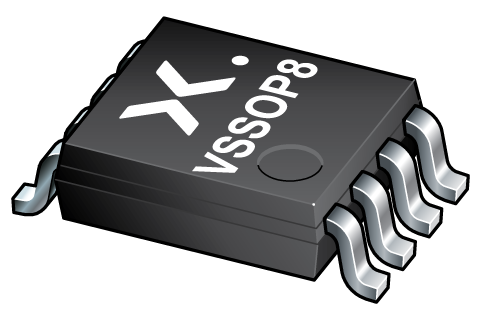 VSSOP8 (SOT765-1) | SOT765-1 | SOT765-1_125 | Active | V74 | 74LVC1G74DC,125 ( 9352 749 73125 ) | |
| 74LVC1G74DP | 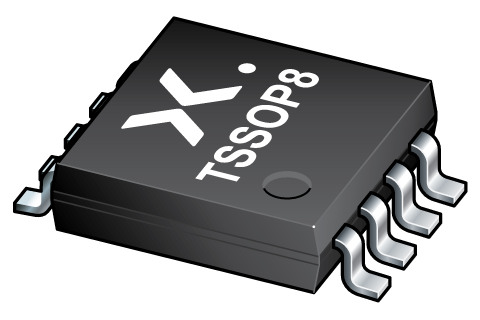 TSSOP8 (SOT505-2) | SOT505-2 | SOT505-2_125 | Active | V74 | 74LVC1G74DP,125 ( 9352 749 74125 ) | |
| 74LVC1G74GN | 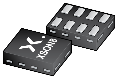 XSON8 (SOT1116) | SOT1116 | REFLOW_BG-BD-1 | SOT1116_115 | Active | Y4 | 74LVC1G74GN,115 ( 9352 922 35115 ) |
| 74LVC1G74GS | 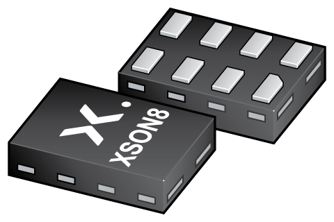 XSON8 (SOT1203) | SOT1203 | REFLOW_BG-BD-1 | SOT1203_115 | Active | Y4 | 74LVC1G74GS,115 ( 9352 927 95115 ) |
| 74LVC1G74GT | 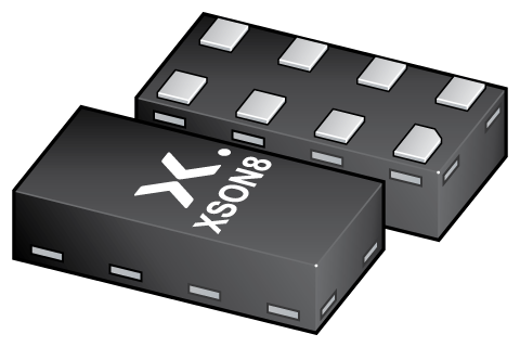 XSON8 (SOT833-1) | SOT833-1 | SOT833-1_115 | Active | V74 | 74LVC1G74GT,115 ( 9352 789 17115 ) |
Environmental information
| Type number | Orderable part number | Chemical content | RoHS | RHF-indicator | Leadfree conversion date |
|---|---|---|---|---|---|
| 74LVC1G74DC | 74LVC1G74DC,125 | 74LVC1G74DC | week 1, 2005 | ||
| 74LVC1G74DP | 74LVC1G74DP,125 | 74LVC1G74DP | week 41, 2004 | ||
| 74LVC1G74GN | 74LVC1G74GN,115 | 74LVC1G74GN | Always Pb-free | ||
| 74LVC1G74GS | 74LVC1G74GS,115 | 74LVC1G74GS | Always Pb-free | ||
| 74LVC1G74GT | 74LVC1G74GT,115 | 74LVC1G74GT | Always Pb-free |
Documentation (15)
| File name | Title | Type | Date |
|---|---|---|---|
| 74LVC1G74 | Single D-type flip-flop with set and reset; positive edge trigger | Data sheet | 2023-08-18 |
| AN10161 | PicoGate Logic footprints | Application note | 2002-10-29 |
| AN11009 | Pin FMEA for LVC family | Application note | 2019-01-09 |
| lvc1g74 | 74LVC1G74 IBIS model | IBIS model | 2014-10-20 |
| Nexperia_Selection_guide_2023 | Nexperia Selection Guide 2023 | Selection guide | 2023-05-10 |
| SOT505-2 | plastic, thin shrink small outline package; 8 leads; 0.65 mm pitch; 3 mm x 3 mm x 1.1 mm body | Package information | 2022-06-03 |
| MAR_SOT1203 | MAR_SOT1203 Topmark | Top marking | 2013-06-03 |
| SOT1203 | plastic, leadless extremely thin small outline package; 8 terminals; 0.35 mm pitch; 1.35 mm x 1 mm x 0.35 mm body | Package information | 2022-06-03 |
| REFLOW_BG-BD-1 | Reflow soldering profile | Reflow soldering | 2021-04-06 |
| MAR_SOT833 | MAR_SOT833 Topmark | Top marking | 2013-06-03 |
| SOT833-1 | plastic, leadless extremely thin small outline package; 8 terminals; 0.5 mm pitch; 1 mm x 1.95 mm x 0.5 mm body | Package information | 2022-06-03 |
| SOT765-1 | plastic, very thin shrink small outline package; 8 leads; 0.5 mm pitch; 2 mm x 2.3 mm x 1 mm body | Package information | 2022-06-03 |
| MAR_SOT1116 | MAR_SOT1116 Topmark | Top marking | 2013-06-03 |
| SOT1116 | plastic, leadless extremely thin small outline package; 8 terminals; 0.3 mm pitch; 1.2 mm x 1 mm x 0.35 mm body | Package information | 2022-06-02 |
| REFLOW_BG-BD-1 | Reflow soldering profile | Reflow soldering | 2021-04-06 |
Support
If you are in need of design/technical support, let us know and fill in the answer form, we'll get back to you shortly.
Models
| File name | Title | Type | Date |
|---|---|---|---|
| lvc1g74 | 74LVC1G74 IBIS model | IBIS model | 2014-10-20 |
Ordering, pricing & availability
Sample
As a Nexperia customer you can order samples via our sales organization or directly via our Online Sample Store: https://extranet.nexperia.com.
Sample orders normally take 2-4 days for delivery.
If you do not have a direct account with Nexperia our network of global and regional distributors is available and equipped to support you with Nexperia samples.