
Features and benefits
-
Wide supply voltage range:
-
VCCI: 0.7 V to 2.75 V
-
VCCO: 1.2 V to 5.5 V
-
-
Low input capacitance; CI = 0.6 pF (typical)
-
Low output capacitance; CO = 1.8 pF (typical)
-
Low dynamic power consumption; CPD = 0.4 pF at VCCI = 1.2 V (typical)
-
Low dynamic power consumption; CPD = 7.1 pF at VCCO = 3.3 V (typical)
-
Low static power consumption; ICCI = 0.5 μA (85 °C maximum)
-
Low static power consumption; ICCO = 1.8 μA (85 °C maximum)
-
High noise immunity
-
Complies with JEDEC standard:
-
JESD8-12A.01 (1.1 V to 1.3 V; A input)
-
JESD8-11A.01 (1.4 V to 1.6 V)
-
JESD8-7A (1.65 V to 1.95 V)
-
JESD8-5A.01 (2.3 V to 2.7 V)
-
JESD8-C (2.7 V to 3.6 V; Y output)
-
JESD12-6 (4.5 V to 5.5 V; Y output)
-
-
ESD protection:
-
HBM ANSI/ESDA/JEDEC JS-001 Class 2 exceeds 2000 V
-
CDM JESD22-C101E exceeds 1000 V
-
-
Latch-up performance exceeds 100 mA per JESD78D Class II
-
Inputs accept voltages up to 2.75 V
-
Low noise overshoot and undershoot < 10% of VCCO
-
IOFF circuitry provides partial power-down mode operation
-
Multiple package options
-
Specified from -40 °C to +85 °C
Parametrics
| Type number | Product status | VCC(A) (V) | VCC(B) (V) | Logic switching levels | Output drive capability (mA) | tpd (ns) | Nr of bits | Power dissipation considerations | Tamb (°C) | Rth(j-a) (K/W) | Ψth(j-top) (K/W) | Rth(j-c) (K/W) | Package name |
|---|---|---|---|---|---|---|---|---|---|---|---|---|---|
| 74AXP1T34GM NRND | Not for design in | 0.7 - 2.75 | 1.2 - 5.5 | CMOS | ± 12 | 4.7 | 1 | ultra low | -40~85 | 305 | 7.3 | 153.6 | XSON6 |
| 74AXP1T34GX NRND | Not for design in | 0.7 - 2.75 | 1.2 - 5.5 | CMOS | ± 12 | 4.7 | 1 | ultra low | -40~85 | 306 | 76.7 | 177 | X2SON5 |
Package
All type numbers in the table below are discontinued. See the table Discontinuation information for more information.
| Type number | Package | Package information | Reflow-/Wave soldering | Packing | Status | Marking | Orderable part number, (Ordering code (12NC)) |
|---|---|---|---|---|---|---|---|
| 74AXP1T34GM | 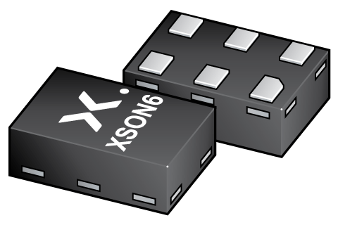 XSON6 (SOT886) | SOT886 | REFLOW_BG-BD-1 | SOT886_125 | Discontinued / End-of-life | rQ | 74AXP1T34GMH ( 9353 069 91125 ) |
| 74AXP1T34GX | 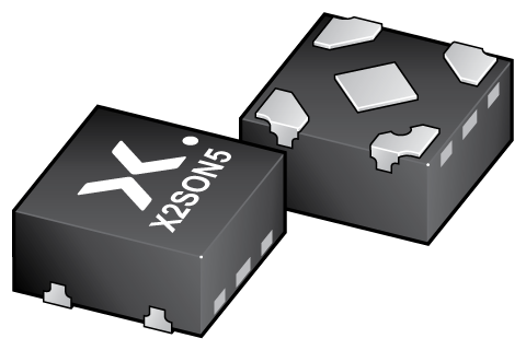 X2SON5 (SOT1226-3) | SOT1226-3 | SOT1226-3_125 | Discontinued / End-of-life | rQ | 74AXP1T34GXH ( 9353 069 95125 ) |
Discontinuation information
| Type number | Orderable part number, (Ordering code (12NC)) | Last time buy date | Last time delivery date | Replacement product | Status | Comments |
|---|---|---|---|---|---|---|
| 74AXP1T34GM | 935306991125 | |||||
| 74AXP1T34GX | 935306995125 |
Environmental information
All type numbers in the table below are discontinued. See the table Discontinuation information for more information.
| Type number | Orderable part number | Chemical content | RoHS | RHF-indicator | Leadfree conversion date |
|---|---|---|---|---|---|
| 74AXP1T34GM | 74AXP1T34GMH | 74AXP1T34GM | Always Pb-free | ||
| 74AXP1T34GX | 74AXP1T34GXH | 74AXP1T34GX | Always Pb-free |
Documentation (11)
| File name | Title | Type | Date |
|---|---|---|---|
| 74AXP1T34 | Dual supply translating buffer | Data sheet | 2022-02-02 |
| AN90029 | Pin FMEA for AXPnT family | Application note | 2021-07-13 |
| Nexperia_document_guide_Logic_translators | Nexperia Logic Translators | Brochure | 2021-04-12 |
| axp1t34 | 74AXP1T34 IBIS model | IBIS model | 2016-04-27 |
| Nexperia_document_leaflet_Logic_X2SON_packages_062018 | X2SON ultra-small 4, 5, 6 & 8-pin leadless packages | Leaflet | 2018-06-05 |
| Nexperia_document_leaflet_Logic_AXP_technology_portfolio_201904 | AXP – Extremely low-power logic technology portfolio | Leaflet | 2019-04-05 |
| Nexperia_Selection_guide_2023 | Nexperia Selection Guide 2023 | Selection guide | 2023-05-10 |
| MAR_SOT886 | MAR_SOT886 Topmark | Top marking | 2013-06-03 |
| SOT886 | plastic, leadless extremely thin small outline package; 6 terminals; 0.5 mm pitch; 1 mm x 1.45 mm x 0.5 mm body | Package information | 2022-06-01 |
| REFLOW_BG-BD-1 | Reflow soldering profile | Reflow soldering | 2021-04-06 |
| SOT1226-3 | plastic thermal enhanced extremely thin small outline package; no leads;5 terminals; body 0.8 x 0.8 x 0.32 mm | Package information | 2020-08-27 |
Support
If you are in need of design/technical support, let us know and fill in the answer form, we'll get back to you shortly.
Models
| File name | Title | Type | Date |
|---|---|---|---|
| axp1t34 | 74AXP1T34 IBIS model | IBIS model | 2016-04-27 |