
Features and benefits
-
Wide supply voltage range for VCC(A) and VCC(B): 0.9 V to 5.5 V
-
Low input capacitance; CI = 1.2 pF (typical)
-
Low output capacitance; CO = 3.6 pF (typical)
-
Low dynamic power consumption; CPD = 10 pF (typical)
-
Low static power consumption; ICC = 2 μA (25 °C maximum)
-
High noise immunity
-
Complies with JEDEC standard:
-
JESD8-12 (1.1 V to 1.3 V; inputs)
-
JESD8-11 (1.4 V to 1.6 V)
-
JESD8-7 (1.65 V to 1.95 V)
-
JESD8-5 (2.3 V to 2.7 V)
-
JESD8C (2.7 V to 3.6 V)
-
JESD12-6 (4.5 V to 5.5 V)
-
-
ESD protection:
-
HBM: ANSI/ESDA/JEDEC JS-001 class 2 exceeds 2 kV
-
CDM: ANSI/ESDA/JEDEC JS-002 class C3 exceeds 1 kV
-
-
Latch-up performance exceeds 100 mA per JESD78D Class II
-
Inputs accept voltages up to 5.5 V
-
Typical data rate figures:
-
320 Mbps when translating from 1.8 V to 3.3 V (up translation)
-
175 Mbps when translating from 3.3 V to 1.8 V (down translation)
-
-
Low noise overshoot and undershoot < 10% of VCCO
-
IOFF circuitry provides partial power-down mode operation
-
Specified from -40 °C to +125 °C
Parametrics
| Type number | Product status | VCC(A) (V) | VCC(B) (V) | Logic switching levels | Output drive capability (mA) | tpd (ns) | Nr of bits | Power dissipation considerations | Tamb (°C) | Rth(j-a) (K/W) | Ψth(j-top) (K/W) | Rth(j-c) (K/W) | Package name |
|---|---|---|---|---|---|---|---|---|---|---|---|---|---|
| 74AXP4T245BQ | Production | 0.9 - 5.5 | 0.9 - 5.5 | CMOS | ± 12 | 9 | 4 | ultra low | -40~125 | 90 | 11.9 | 60 | DHVQFN16 |
| 74AXP4T245PW | Production | 0.9 - 5.5 | 0.9 - 5.5 | CMOS | ± 12 | 9 | 4 | ultra low | -40~125 | 123 | 4.0 | 52 | TSSOP16 |
Package
| Type number | Package | Package information | Reflow-/Wave soldering | Packing | Status | Marking | Orderable part number, (Ordering code (12NC)) |
|---|---|---|---|---|---|---|---|
| 74AXP4T245BQ | 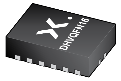 DHVQFN16 (SOT763-1) | SOT763-1 | SOT763-1_115 | Active | P4T245 | 74AXP4T245BQX ( 9356 907 04115 ) | |
| 74AXP4T245PW | 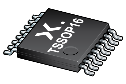 TSSOP16 (SOT403-1) | SOT403-1 | SSOP-TSSOP-VSO-WAVE | SOT403-1_118 | Active | XP4T245 | 74AXP4T245PWJ ( 9356 907 03118 ) |
Environmental information
| Type number | Orderable part number | Chemical content | RoHS | RHF-indicator | Leadfree conversion date |
|---|---|---|---|---|---|
| 74AXP4T245BQ | 74AXP4T245BQX | 74AXP4T245BQ | week 25, 2019 | ||
| 74AXP4T245PW | 74AXP4T245PWJ | 74AXP4T245PW | week 25, 2019 |
Documentation (7)
| File name | Title | Type | Date |
|---|---|---|---|
| 74AXP4T245 | 4-bit dual supply translating transceiver; 3-state | Data sheet | 2020-02-06 |
| AN90029 | Pin FMEA for AXPnT family | Application note | 2021-07-13 |
| axp4t245 | 74AXP4T245 IBIS model | IBIS model | 2020-11-20 |
| Nexperia_Selection_guide_2023 | Nexperia Selection Guide 2023 | Selection guide | 2023-05-10 |
| SOT763-1 | plastic, leadless dual in-line compatible thermal enhanced very thin quad flat package; 16 terminals; 0.5 mm pitch; 3.5 mm x 2.5 mm x 1 mm body | Package information | 2023-05-11 |
| SOT403-1 | plastic, thin shrink small outline package; 16 leads; 5 mm x 4.4 mm x 1.2 mm body | Package information | 2023-11-08 |
| SSOP-TSSOP-VSO-WAVE | Footprint for wave soldering | Wave soldering | 2009-10-08 |
Support
If you are in need of design/technical support, let us know and fill in the answer form, we'll get back to you shortly.
Models
| File name | Title | Type | Date |
|---|---|---|---|
| axp4t245 | 74AXP4T245 IBIS model | IBIS model | 2020-11-20 |
Ordering, pricing & availability
Sample
As a Nexperia customer you can order samples via our sales organization or directly via our Online Sample Store: https://extranet.nexperia.com.
Sample orders normally take 2-4 days for delivery.
If you do not have a direct account with Nexperia our network of global and regional distributors is available and equipped to support you with Nexperia samples.