
Features and benefits
-
Wide supply voltage range of 2.3 V to 3.6 V
-
CMOS low power consumption
-
MULTIBYTE™ flow-through standard pin-out architecture
-
Low inductance multiple VCC and GND pins for minimize noise and ground bounce
-
Bushold on all data inputs(74ALVCH16245 only)
-
Current drive ±24 mA at VCC = 3.0 V.
-
Direct interface with TTL levels
-
Output drive capability 50 Ω transmission lines at 85 °C
-
Complies with JEDEC standards:
-
JESD8-7 (1.65 V to 1.95 V)
-
JESD8-5 (2.3 V to 2.7 V)
-
JESD8C/JESD36 (2.7 V to 3.6 V)
-
-
ESD protection:
- HBM ANSI/ESDA/JEDEC JS-001 Class 2 exceeds 2 kV
- CDM ANSI/ESDA/JEDEC JS-002 Class C3 exceeds 1 kV
-
Specified from -40 °C to +85 °C and from -40 °C to +125 °C
Parametrics
| Type number | Product status | VCC(A) (V) | VCC(B) (V) | Logic switching levels | Output drive capability (mA) | tpd (ns) | Nr of bits | fmax (MHz) | Power dissipation considerations | Tamb (°C) | Rth(j-a) (K/W) | Package name |
|---|---|---|---|---|---|---|---|---|---|---|---|---|
| 74ALVCH16646DGG | Production | n.a. | n.a. | TTL | ± 24 | 2.6 | 16 | 150 | low | -40~85 | 93 | TSSOP56 |
Package
| Type number | Package | Package information | Reflow-/Wave soldering | Packing | Status | Marking | Orderable part number, (Ordering code (12NC)) |
|---|---|---|---|---|---|---|---|
| 74ALVCH16646DGG | 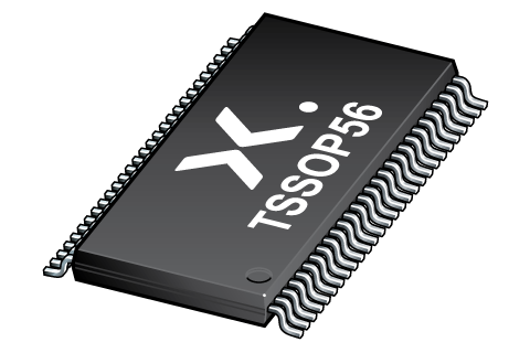 TSSOP56 (SOT364-1) | SOT364-1 | SSOP-TSSOP-VSO-WAVE | SOT364-1_118 | Active | ALVCH16646 | 74ALVCH16646DGG:11 ( 9352 624 21118 ) |
The variants in the table below are discontinued. See the table Discontinuation information for more information.
| Type number | Package | Package information | Reflow-/Wave soldering | Packing | Status | Marking | Orderable part number, (Ordering code (12NC)) |
|---|---|---|---|---|---|---|---|
| 74ALVCH16646DGG | TSSOP56 (SOT364-1) | SOT364-1 | SSOP-TSSOP-VSO-WAVE | SOT364-1_518 | Discontinued / End-of-life | ALVCH16646 | 74ALVCH16646DGGY ( 9352 624 21518 ) |
Discontinuation information
| Type number | Orderable part number, (Ordering code (12NC)) | Last time buy date | Last time delivery date | Replacement product | Status | Comments |
|---|---|---|---|---|---|---|
| 74ALVCH16646DGG | 935262421518 | |||||
| 74ALVCH16646DGG | 935262421512 | 2021-12-31 | 2022-06-30 | 74ALVCH16646DGG | ||
| 74ALVCH16646DGG | 935262421112 |
Environmental information
| Type number | Orderable part number | Chemical content | RoHS | RHF-indicator | Leadfree conversion date |
|---|---|---|---|---|---|
| 74ALVCH16646DGG | 74ALVCH16646DGG:11 | 74ALVCH16646DGG | week 2, 2006 |
The variants in the table below are discontinued. See the table Discontinuation information for more information.
| Type number | Orderable part number | Chemical content | RoHS | RHF-indicator | Leadfree conversion date |
|---|---|---|---|---|---|
| 74ALVCH16646DGG | 74ALVCH16646DGGY | 74ALVCH16646DGG | Always Pb-free |
Documentation (5)
| File name | Title | Type | Date |
|---|---|---|---|
| 74ALVCH16646 | 16-bit bus transceiver/register; 3-state | Data sheet | 2018-09-11 |
| alvch16646 | alvch16646 IBIS model | IBIS model | 2013-04-07 |
| Nexperia_Selection_guide_2023 | Nexperia Selection Guide 2023 | Selection guide | 2023-05-10 |
| SSOP-TSSOP-VSO-WAVE | Footprint for wave soldering | Wave soldering | 2009-10-08 |
| SOT364-1 | plastic, thin shrink small outline package; 56 leads; 0.5 mm pitch; 14 mm x 6.1 mm x 1.2 mm body | Package information | 2022-06-23 |
Support
If you are in need of design/technical support, let us know and fill in the answer form, we'll get back to you shortly.
Models
| File name | Title | Type | Date |
|---|---|---|---|
| alvch16646 | alvch16646 IBIS model | IBIS model | 2013-04-07 |
Ordering, pricing & availability
Sample
As a Nexperia customer you can order samples via our sales organization or directly via our Online Sample Store: https://extranet.nexperia.com.
Sample orders normally take 2-4 days for delivery.
If you do not have a direct account with Nexperia our network of global and regional distributors is available and equipped to support you with Nexperia samples.