Orderable parts
| Type number | Orderable part number | Ordering code (12NC) | Package | Buy from distributors |
|---|---|---|---|---|
| 74AXP8T245BQ | 74AXP8T245BQJ | 935690813118 | SOT815-1 | Order product |
Register once, drag and drop ECAD models into your CAD tool and speed up your design.
Click here for more information8-bit dual supply translating transceiver; 3-state
The 74AXP8T245 is an 8-bit dual supply translating transceiver with 3-state outputs that enable bidirectional level translation. It features two data input-output ports (pins An and Bn), a direction control input (DIR), an output enable input (OE) and dual supply pins (VCC(A) and VCC(B)). Both VCC(A) and VCC(B) can be supplied at any voltage between 0.9 V and 5.5 V making the device suitable for translating between any of the low voltage nodes (0.9 V, 1.2 V, 1.5 V, 1.8 V, 2.5 V, 3.3 V and 5.0 V). No power supply sequencing is required and output glitches during power supply transitions are prevented using patented circuitry. As a result glitches will not appear on the outputs for supply transitions during power-up/down between 20 mV/µs and 5.5 V/s.
Pins An, OE and DIR are referenced to VCC(A) and pins Bn are referenced to VCC(B). A HIGH on DIR allows transmission from An to Bn and a LOW on DIR allows transmission from Bn to An. The output enable input (OE) can be used to disable the outputs so the buses are effectively isolated.
The devices are fully specified for partial power-down applications using IOFF. The IOFF circuitry disables the output, preventing any damaging backflow current through the device when it is powered down. In suspend mode when either VCC(A) or VCC(B) are at GND level, both An and Bn are in the high-impedance OFF-state.
Wide supply voltage range:
VCC(A): 0.9 V to 5.5 V
VCC(B): 0.9 V to 5.5 V
Low input capacitance; CI = 1.5 pF (typical)
Low output capacitance; CO = 3.8 pF (typical)
Low dynamic power consumption; CPD = 10 pF (typical)
Low static power consumption; ICC = 2 μA (25 °C maximum)
High noise immunity
Complies with JEDEC standard:
JESD8-12 (1.1 V to 1.3 V; inputs)
JESD8-11 (1.4 V to 1.6 V)
JESD8-7 (1.65 V to 1.95 V)
JESD8-5 (2.3 V to 2.7 V)
JESD8C (2.7 V to 3.6 V)
JESD12-6 (4.5 V to 5.5 V)
ESD protection:
HBM: ANSI/ESDA/JEDEC JS-001 class 2 exceeds 2000 V
CDM: ANSI/ESDA/JEDEC JS-002 class C3 exceeds 1000 V
Latch-up performance exceeds 100 mA per JESD78D Class II
Inputs accept voltages up to 5.5 V
Low noise overshoot and undershoot < 10% of VCCO
IOFF circuitry provides partial power-down mode operation
Specified from -40 °C to +125 °C
| Type number | Product status | VCC(A) (V) | VCC(B) (V) | Logic switching levels | Output drive capability (mA) | tpd (ns) | Nr of bits | Power dissipation considerations | Tamb (°C) | Rth(j-a) (K/W) | Ψth(j-top) (K/W) | Rth(j-c) (K/W) | Package name |
|---|---|---|---|---|---|---|---|---|---|---|---|---|---|
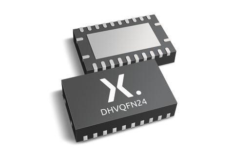
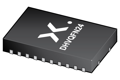
| 74AXP8T245BQ | Production | 0.9 - 5.5 | 0.9 - 5.5 | CMOS | ± 12 | 9 | 4 | ultra low | -40~125 | 68 | 6.4 | 42 | DHVQFN24 |
| Type number | Orderable part number, (Ordering code (12NC)) | Status | Marking | Package | Package information | Reflow-/Wave soldering | Packing |
|---|---|---|---|---|---|---|---|
| 74AXP8T245BQ | 74AXP8T245BQJ (935690813118) |
Active | AXP8T245 |
DHVQFN24 (SOT815-1) |
SOT815-1 | SOT815-1_118 |
| Type number | Orderable part number | Chemical content | RoHS | RHF-indicator |
|---|---|---|---|---|
| 74AXP8T245BQ | 74AXP8T245BQJ | 74AXP8T245BQ |
|
|
| File name | Title | Type | Date |
|---|---|---|---|
| 74AXP8T245 | 8-bit dual supply translating transceiver; 3-state | Data sheet | 2020-02-11 |
| AN90029 | Pin FMEA for AXPnT family | Application note | 2021-07-13 |
| SOT815-1 | 3D model for products with SOT815-1 package | Design support | 2019-10-03 |
| Nexperia_document_leaflet_Logic_AXP_technology_portfolio_201904 | AXP – Extremely low-power logic technology portfolio | Leaflet | 2019-04-05 |
| Nexperia_package_poster | Nexperia package poster | Leaflet | 2020-05-15 |
| DHVQFN24_SOT815-1_mk | plastic, dual in-line compatible thermal enhanced very thin quad flat package; 24 terminals; 0.5 mm pitch; 3.5 mm x 5.5 mm x 0.85 mm body | Marcom graphics | 2017-01-28 |
| SOT815-1 | plastic, leadless dual in-line compatible thermal enhanced very thin quad flat package; 24 terminals; 0.5 mm pitch; 5.5 mm x 3.5 mm x 1 mm body | Package information | 2021-08-17 |
| SOT815-1_118 | DHVQFN24; Reel pack for SMD, 13"; Q1/T1 product orientation | Packing information | 2020-04-21 |
| 74AXP8T245BQ_Nexperia_Product_Reliability | 74AXP8T245BQ Nexperia Product Reliability | Quality document | 2023-05-29 |
If you are in need of design/technical support, let us know and fill in the answer form we'll get back to you shortly.
| File name | Title | Type | Date |
|---|---|---|---|
| SOT815-1 | 3D model for products with SOT815-1 package | Design support | 2019-10-03 |
| Type number | Orderable part number | Ordering code (12NC) | Status | Packing | Packing Quantity | Buy online |
|---|---|---|---|---|---|---|
| 74AXP8T245BQ | 74AXP8T245BQJ | 935690813118 | Active | SOT815-1_118 | 3,000 | Order product |
As a Nexperia customer you can order samples via our sales organization or directly via our Online Sample Store: https://extranet.nexperia.com.
Sample orders normally take 2-4 days for delivery.
If you do not have a direct account with Nexperia our network of global and regional distributors is available and equipped to support you with Nexperia samples.
The interactive datasheets are based on the Nexperia MOSFET precision electrothermal models. With our interactive datasheets you can simply specify your own conditions interactively. Start by changing the values of the conditions. You can do this by using the sliders in the condition fields. By dragging the sliders you will see how the MOSFET will perform at the new conditions set.
8-bit dual supply translating transceiver; 3-state
| SKU | Stock* | MOQ | Price per unit | Quantity |
|---|
| Seller | SKU | Stock | MOQ | 1 | 10 | 100 | 1,000 | 10,000 | Purchase |
|---|
| Seller | SKU | Stock | MOQ | 1 | 10 | 100 | 1,000 | 10,000 | Purchase |
|---|
| Seller | SKU | Stock | MOQ | 1 | 10 | 100 | 1,000 | 10,000 | Purchase |
|---|
| Seller | SKU | Stock | MOQ | 1 | 10 | 100 | 1,000 | 10,000 | Purchase |
|---|
| Seller | SKU | Stock | MOQ | 1 | 10 | 100 | 1,000 | 10,000 | Purchase |
|---|