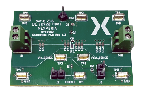
NEVB-NPS1000 load switch evaluation board
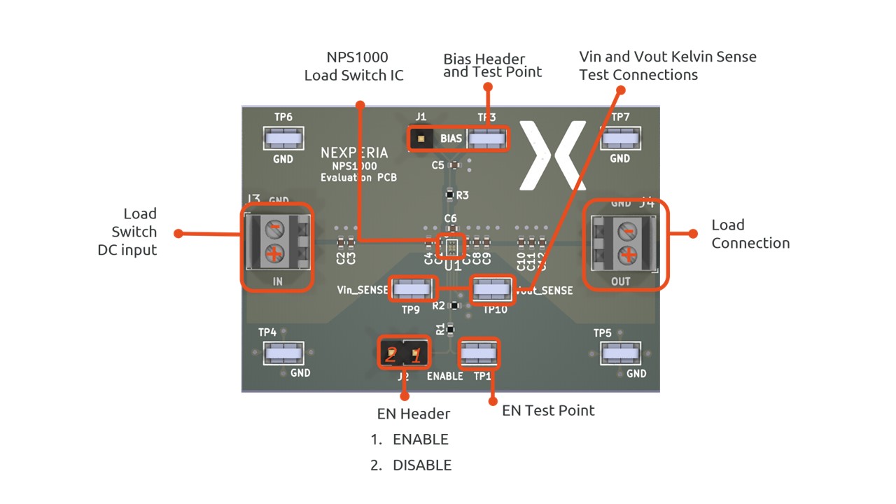
The NEVB-NPS1000 is a two-layer PCB containing the NPS1000 load switch device. The VIN and VOUT connections to the device and the PCB layout routing provides a low-resistance pathway into and out of the device under test. Test point connections allow the EVB user to control the device with userdefined test conditions a nd make accurate device measurements.
Key features and benefits
• Input operating voltage range (VIN): 0.5 V to 1 V
• Rated currents: 0.6A RMS, 1.5A peak
• ON resistance (RDS(on)): 11 mΩ (typical) at 25C
• Controlled Startup
• <200us from enable to full enhancement of power FET
• Output short tolerant
• When supplied by a 4.5A current limited power supply
• Over-Temperature Shutdown and Input UVLO Protection
• 8Ω Discharge While Disabled
• WLCSP package footprint
• Convenient connections via test points and INPUT/OUTPUT terminals
Products on the board (1)
| Type number | Description | Status | Quick access | |
|---|---|---|---|---|
|
NPS1000UP | 0.5 V to 1.0 V, 1.5 A peak, 11 mΩ, load switch | Production |
Products on the board (1)
| Type number | Description | Status | Quick access | |
|---|---|---|---|---|
|
|
NPS1000UP | 0.5 V to 1.0 V, 1.5 A peak, 11 mΩ, load switch | Production |
Documentation (2)
Support
If you are in need of design/technical support, let us know and fill in the answer form, we'll get back to you shortly.