
Features and benefits
-
Automotive product qualification in accordance with AEC-Q100 (Grade 1)
- Specified from -40 °C to +85 °C and from -40 °C to +125 °C
-
Wide operating range: 1.5 V to 5.5 V
-
2x SP4T-Z functionality
-
Rail-to-Rail operation on analog signal pins
-
Injection current control
-
1.8 V digital logic thresholds
-
Digital pins compatible with 1.8 V logic thresholds across full VCC range
-
Removes need for up-translation device for compatibility with low voltage GPIOs
-
-
Ioff circuitry
-
Enables wider latitude for power sequencing considerations
-
Isolates backflow between supply rail and any biased digital/analog input when VCC = 0 V
-
Prevents any biased digital/analog input from backpowering VCC when VCC = 0 V
-
Maintains Hi-Z state of analog switch when VCC = 0 V
-
-
5.5 V overvoltage tolerant digital inputs
-
Supports switching of 5.5 V digital signals across full VCC operating range
-
Removes need for down-translation when switching thresholds are met
-
-
Pin compatible with industry standard 4052 and 4852 analog switch products
-
ESD protection:
-
HBM: ANSI/ESDA/JEDEC JS-001 class 2 exceeds 2000 V
-
CDM: ANSI/ESDA/JEDEC JS-002 class C2b exceeds 750 V
-
-
DHVQFN package with Side-Wettable Flanks enabling Automatic Optical Inspection (AOI) of solder joints
Applications
-
Body control module
-
Battery management system
-
Automotive head unit
Parametrics
| Type number | Product status | Configuration | VCC (V) | RON (Ω) | RON(FLAT) (Ω) | Logic switching levels | Power dissipation considerations | Tamb (°C) | Rth(j-a) (K/W) | Ψth(j-top) (K/W) | Rth(j-c) (K/W) | Package name |
|---|---|---|---|---|---|---|---|---|---|---|---|---|
| NMUX1309BQ-Q100 | Production | SP4T-Z | 1.5 - 5.5 | 60 | - | CMOS | very low | -40~125 | 93 | 62.0 | 13.8 | DHVQFN16 |
| NMUX1309PW-Q100 | Production | SP4T-Z | 1.5 - 5.5 | 60 | - | CMOS | very low | -40~125 | 139 | 64.0 | 6.9 | TSSOP16 |
(-) dash denotes: "Parameter value not specified for this product"
Package
| Type number | Package | Package information | Reflow-/Wave soldering | Packing | Status | Marking | Orderable part number, (Ordering code (12NC)) |
|---|---|---|---|---|---|---|---|
| NMUX1309BQ-Q100 | 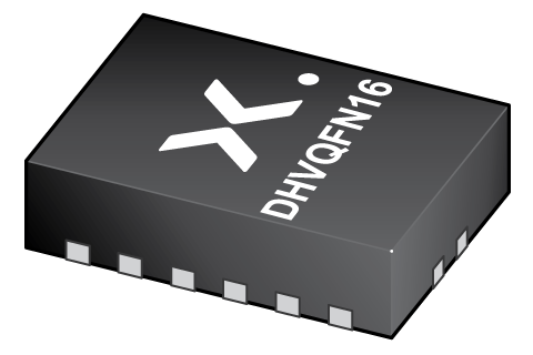 DHVQFN16 (SOT763-1) | SOT763-1 | SOT763-1_115 | Active | NM1309 | NMUX1309BQ-Q100X ( 9356 914 16115 ) | |
| NMUX1309PW-Q100 | 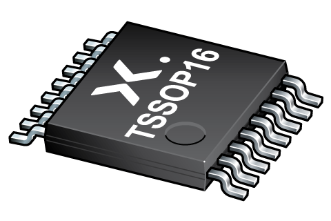 TSSOP16 (SOT403-1) | SOT403-1 | SSOP-TSSOP-VSO-WAVE | SOT403-1_118 | Active | NMU1309 | NMUX1309PW-Q100J ( 9356 914 18118 ) |
Environmental information
| Type number | Orderable part number | Chemical content | RoHS | RHF-indicator | Leadfree conversion date |
|---|---|---|---|---|---|
| NMUX1309BQ-Q100 | NMUX1309BQ-Q100X | NMUX1309BQ-Q100 | |||
| NMUX1309PW-Q100 | NMUX1309PW-Q100J | NMUX1309PW-Q100 |
Documentation (7)
| File name | Title | Type | Date |
|---|---|---|---|
| NMUX1309_Q100 | 1.5 V to 5.5 V, dual 4-channel switch analog multiplexer and demultiplexer with injection-current control | Data sheet | 2024-04-16 |
| AN90051 | Pin FMEA for NMUX130x family | Application note | 2024-02-13 |
| 1_8V_General_purpose_injection_control_analog_switch_leaflet | 1.8 V General purpose SP8T-Z and 2x SP4T-Z analog switches with injection current control | Leaflet | 2024-03-05 |
| UM90026 | NMUX1308; NMUX1309 evaluation board | User manual | 2024-01-18 |
| SOT763-1 | plastic, leadless dual in-line compatible thermal enhanced very thin quad flat package; 16 terminals; 0.5 mm pitch; 3.5 mm x 2.5 mm x 1 mm body | Package information | 2023-05-11 |
| SOT403-1 | plastic, thin shrink small outline package; 16 leads; 5 mm x 4.4 mm x 1.2 mm body | Package information | 2023-11-08 |
| SSOP-TSSOP-VSO-WAVE | Footprint for wave soldering | Wave soldering | 2009-10-08 |
Support
If you are in need of design/technical support, let us know and fill in the answer form, we'll get back to you shortly.
Ordering, pricing & availability
Sample
As a Nexperia customer you can order samples via our sales organization or directly via our Online Sample Store: https://extranet.nexperia.com.
Sample orders normally take 2-4 days for delivery.
If you do not have a direct account with Nexperia our network of global and regional distributors is available and equipped to support you with Nexperia samples.