


Block diagram
Products - Power
Design challenges
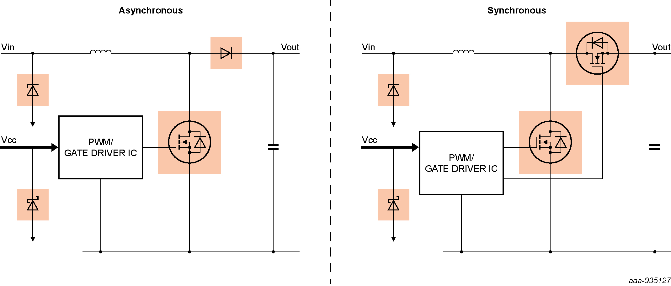
- Point of load non-isolated DC/DC boost converter circuit
- Economical, two-MOSFET design - low QG(tot) and low FOM for best efficiency
- Easily switch from asynchronous to synchronous conversion depending on choice of high-side diode or MOSFET
- Lower switch losses improve thermal behaviour
- LFPAK and CFP (both clip-bond package) allow a high-efficiency DCDC converter solutions, while reducing costs (less heating to dissipate)
- Possibility to go to higher switching frequency (FSW), which leads to smaller inductances and smaller capacitors
- Best thermal performance thanks to clip-bonding package
MOSFET and GaN FET Handbook
Drawing on over 20 years’ of experience, the MOSFET and GaN FET Application Handbook: A Power Design Engineer’s Guide brings together a comprehensive set of learning and reference materials relating to the use of MOSFETs and GaN FETs in real world systems.

Let us help you with product and design questions
Contact our technical support desk for your technical questions.