


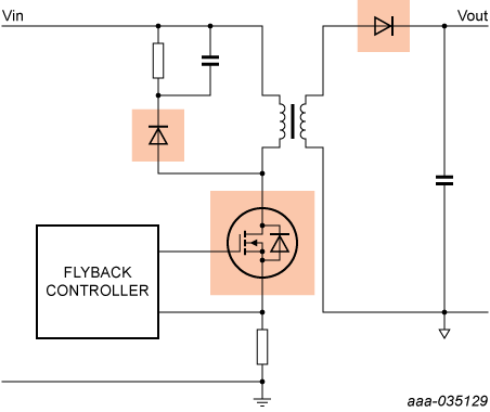
Block diagram
Products - Power
Nexperia value proposition
- Lower switch losses improve even more the thermal behaviour
- LFPAK and CFP (both clip-bond package) allow a high-efficiency DC/DC converter solutions, while reducing costs (less heating to dissipate)
- Standard packages MLPAK33 and MLPAK56 also available
- Therefore the possibility to go to higher switching frequency (FSW), which leads to smaller inductances and smaller capacities
- Best thermal performance thanks to clip-bond package - Rth 3x better than competition - and SiGe diodes that have no thermal runaway
MOSFET and GaN FET Handbook
Drawing on over 20 years’ of experience, the MOSFET and GaN FET Application Handbook: A Power Design Engineer’s Guide brings together a comprehensive set of learning and reference materials relating to the use of MOSFETs and GaN FETs in real world systems.

Let us help you with product and design questions
Contact our technical support desk for your technical questions.