


NXU0304
4-bit dual-supply voltage level translating buffer with Schmitt-trigger; 3-state
The NXU0304 is a 4-bit, dual-supply level translating buffer with Schmitt-trigger inputs and 3-state outputs. It features four data inputs (An and B4), four data outputs (YBn and YA4) and an output enable input (OE).
Both VCCA and VCCB can be supplied at any voltage between 0.9 V and 5.5 V making the device suitable for translating between any of the voltage nodes (1.2 V, 1.5 V, 1.8 V, 2.5 V, 3.3 V and 5.0 V).
This device facilitates asynchronous communication between data buses. Transmit data with a fixed direction (unidirectionally) from the A bus to the B bus on three channels and from the B bus to the A bus for on one channel. The OE pin can be referenced to VCCA and VCCB domain and when OE pin is set LOW the outputs are disabled and enter a high-impedance OFF-state which isolates the buses. The OE pin can be left floating or externally pulled down to ground to ensure the high-impedance state of the outputs during power up or power down.
This device ensures low static and dynamic power consumption across the entire supply range and is fully specified for partial power down applications using IOFF. The IOFF circuitry prevents potentially damaging backflow current through the device when it is powered down or if one of the power supplies is disconnected (floating).
No power supply sequencing is required and output glitches during power supply transitions are prevented. As a result, glitches will not appear on the outputs for supply transitions during power-up/down.
 |
Features and benefits
Wide supply voltage range:
VCCA: 0.9 V to 5.5 V
VCCB: 0.9 V to 5.5 V
- Low power consumption for supply voltage range 1.1 V to 5.5 V
- 3 µA (Tamb = 25 °C)
- 5 µA (Tamb = -40 °C to +125 °C)
- Schmitt-trigger inputs with integrated static high ohmic pull-down resistor on the input
Maximum data rates:
250 Mbps (≥ 1.8 V to 5 V translation)
High output drive 12 mA at 5 V
Output enable (OE) allows connection to VCCA or VCCB domain
Suspend mode when either one of the supply voltages is below 100 mV or disconnected (floating)
Low noise overshoot and undershoot <10% of VCCO
IOFF circuitry provides partial power-down mode operation
Latch-up performance exceeds 100 mA per JESD78D Class II
Complies with JEDEC standard:
JESD8-12 (0.9 V to 1.3 V)
JESD8-11 (1.4 V to 1.6 V)
JESD8-7 (1.65 V to 1.95 V)
JESD8-5 (2.3 V to 2.7 V)
JESD8C (2.7 V to 3.6 V)
JESD12-6 (4.5 V to 5.5 V)
ESD protection:
HBM: ANSI/ESDA/JEDEC JS-001 class 2 exceeds 2500 V
CDM: ANSI/ESDA/JEDEC JS-002 class C3 exceeds 1500 V
Specified from -40 °C to +85 °C and -40 °C to +125 °C
Similar functions: NXU0104 and NXU0204
Applications
- General purpose I/O level translation
- Noisy environments or slow input signals
- Supports push-pull voltage translation as UART, SPI and JTAG protocols
- Consumer
Parametrics
| Type number | Logic switching levels | Output drive capability (mA) | Nr of bits | Power dissipation considerations | Tamb (°C) | Rth(j-a) (K/W) | Ψth(j-top) (K/W) | Rth(j-c) (K/W) | Package name |
|---|---|---|---|---|---|---|---|---|---|
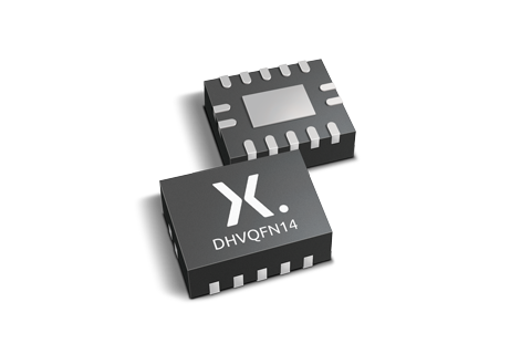
| NXU0304BQ | CMOS/LVTTL | ± 12 | 4 | ultra low | -40~125 | 98 | 14 | 65 | DHVQFN14 |
| NXU0304BQ-Q100 | CMOS/LVTTL | ± 12 | 4 | ultra low | -40~125 | 98 | 14 | 65 | DHVQFN14 |
| NXU0304BZ | CMOS/LVTTL | ± 12 | 4 | ultra low | -40~125 | 98 | 3.4 | 71 | DHXQFN14 |
| NXU0304GU12 | CMOS/LVTTL | ± 12 | 4 | ultra low | -40~125 | 172 | 3.3 | 82 | XQFN12 |
| NXU0304GU12-Q100 | CMOS/LVTTL | ± 12 | 4 | ultra low | -40~125 | 172 | 3.3 | 82 | XQFN12 |
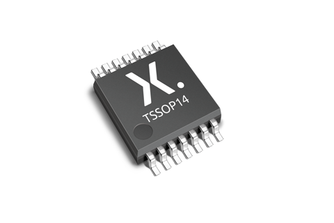
| NXU0304PW | CMOS/LVTTL | ± 12 | 4 | ultra low | -40~125 | 134 | 3.3 | 59 | TSSOP14 |
| NXU0304PW-Q100 | CMOS/LVTTL | ± 12 | 4 | ultra low | -40~125 | 134 | 3.3 | 59 | TSSOP14 |
Package
| Type number | Orderable part number, (Ordering code (12NC)) | Status | Marking | Package | Package information | Reflow-/Wave soldering | Packing |
|---|---|---|---|---|---|---|---|
| NXU0304BQ | NXU0304BQX (935691848115) |
Active | U0304 |
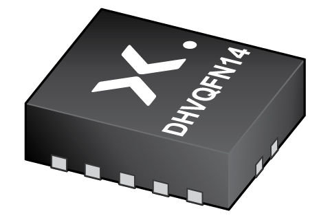
DHVQFN14 (SOT762-1) |
SOT762-1 | SOT762-1_115 | |
| NXU0304BQ-Q100 | NXU0304BQ‑Q100X (935691851115) |
Active | U0304 |
DHVQFN14 (SOT762-1) |
SOT762-1 | SOT762-1_115 | |
| NXU0304BZ | NXU0304BZZ (935691849147) |
Active | L03 |
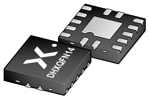
DHXQFN14 (SOT8014-1) |
SOT8014-1 | SOT8014-1_147 | |
| NXU0304GU12 | NXU0304GU12X (935691850115) |
Active | L6 |
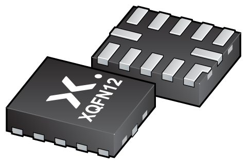
XQFN12 (SOT1174-1) |
SOT1174-1 | SOT1174-1_115 | |
| NXU0304GU12-Q100 | NXU0304GU12‑Q100X (935691853115) |
Active | L6 |
XQFN12 (SOT1174-1) |
SOT1174-1 | SOT1174-1_115 | |
| NXU0304PW | NXU0304PWJ (935691842118) |
Active | NXU0304 |
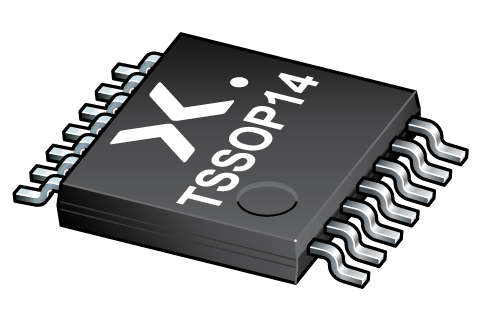
TSSOP14 (SOT402-1) |
SOT402-1 |
SSOP-TSSOP-VSO-WAVE
|
SOT402-1_118 |
| NXU0304PW-Q100 | NXU0304PW‑Q100J (935691847118) |
Active | NXU0304 |
TSSOP14 (SOT402-1) |
SOT402-1 |
SSOP-TSSOP-VSO-WAVE
|
SOT402-1_118 |
Environmental information
| Type number | Orderable part number | Chemical content | RoHS | RHF-indicator |
|---|---|---|---|---|
| NXU0304BQ | NXU0304BQX | NXU0304BQ |
|
|
| NXU0304BQ-Q100 | NXU0304BQ‑Q100X | NXU0304BQ-Q100 |
|
|
| NXU0304BZ | NXU0304BZZ | NXU0304BZ |
|
|
| NXU0304GU12 | NXU0304GU12X | NXU0304GU12 |
|
|
| NXU0304GU12-Q100 | NXU0304GU12‑Q100X | NXU0304GU12-Q100 |
|
|
| NXU0304PW | NXU0304PWJ | NXU0304PW |
|
|
| NXU0304PW-Q100 | NXU0304PW‑Q100J | NXU0304PW-Q100 |
|
|
Documentation (17)
| File name | Title | Type | Date |
|---|---|---|---|
| NXU0304 | 4-bit dual-supply voltage level translating buffer with Schmitt-trigger; 3-state | Data sheet | 2024-12-02 |
| AN90057 | Pin FMEA for NXU family | Application note | 2024-09-11 |
| AN90063 | Questions about package outline drawings | Application note | 2025-10-22 |
| SOT762-1 | 3D model for products with SOT762-1 package | Design support | 2019-10-03 |
| SOT8014-1 | 3D model for products with SOT8014-1 package | Design support | 2023-02-02 |
| SOT1174-1 | 3D model for products with SOT1174-1 package | Design support | 2021-01-28 |
| SOT402-1 | 3D model for products with SOT402-1 package | Design support | 2023-02-02 |
| nxu0304 | NXU0304 IBIS model | IBIS model | 2024-09-03 |
| Nexperia_package_poster | Nexperia package poster | Leaflet | 2020-05-15 |
| DHVQFN14_SOT762-1_mk | plastic, dual in-line compatible thermal enhanced very thin quad flat package; no leads; 14 terminals; 0.5 mm pitch; 2.5 mm x 3 mm x 0.85 mm body | Marcom graphics | 2017-01-28 |
| TSSOP14_SOT402-1_mk | plastic, thin shrink small outline package; 14 leads; 0.65 mm pitch; 5 mm x 4.4 mm x 1.1 mm body | Marcom graphics | 2017-01-28 |
| SOT762-1 | plastic, leadless dual in-line compatible thermal enhanced very thin quad flat package; 14 terminals; 0.5 mm pitch; 2.5 x 3 x 1 mm body | Package information | 2023-04-05 |
| SOT8014-1 | plastic, leadless dual in-line compatible thermal enhanced extreme thin quad flat package;no leads; 14 terminals; 0.4 mm pitch; body 2 mm x 2 mm x 0.48 mm | Package information | 2023-02-28 |
| SOT1174-1 | plastic, leadless extremely thin quad flat package; 12 terminals; 0.4 mm pitch; 2 mm x 1.7 mm x 0.5 mm body | Package information | 2024-04-11 |
| SOT402-1 | plastic, thin shrink small outline package; 14 leads; 0.65 mm pitch; 5 mm x 4.4 mm x 1.2 mm body | Package information | 2023-11-07 |
| UM90041 | NXU0104, NXU0204 and NXU0304 evaluation board | User manual | 2024-09-11 |
| SSOP-TSSOP-VSO-WAVE | Footprint for wave soldering | Wave soldering | 2009-10-08 |
Support
If you are in need of design/technical support, let us know and fill in the answer form we'll get back to you shortly.
Models
| File name | Title | Type | Date |
|---|---|---|---|
| SOT762-1 | 3D model for products with SOT762-1 package | Design support | 2019-10-03 |
| SOT8014-1 | 3D model for products with SOT8014-1 package | Design support | 2023-02-02 |
| SOT1174-1 | 3D model for products with SOT1174-1 package | Design support | 2021-01-28 |
| SOT402-1 | 3D model for products with SOT402-1 package | Design support | 2023-02-02 |
| nxu0304 | NXU0304 IBIS model | IBIS model | 2024-09-03 |
Ordering, pricing & availability
Sample
As a Nexperia customer you can order samples via our sales organization.
If you do not have a direct account with Nexperia our network of global and regional distributors is available and equipped to support you with Nexperia samples. Check out the list of official distributors.