


74CBTLV3253
Dual 1-of-4 multiplexer/demultiplexer
The 74CBTLV3253 provides a dual 1-of-4 high-speed multiplexer/demultiplexer with two common select inputs (S0, S1) and two output enable inputs (1OE, 2OE). The low ON resistance of the switch allows inputs to be connected to outputs without adding propagation delay or generating additional ground bounce noise. When pin nOE = LOW, one of the four switches is selected (low-impedance ON-state) with pins S0 and S1. When pin nOE = HIGH, all switches are in the high-impedance OFF-state, independent of pins S0 and S1.
To ensure the high-impedance OFF-state during power-up or power-down, nOE should be tied to the VCC through a pull-up resistor. The minimum value of the resistor is determined by the current-sinking capability of the driver.
Schmitt trigger action at control input makes the circuit tolerant to slower input rise and fall times across the entire VCC range from 2.3 V to 3.6 V.
This device is fully specified for partial power-down applications using IOFF. The IOFF circuitry disables the output, preventing the damaging backflow current through the device when it is powered down.
Features and benefits
Supply voltage range from 2.3 V to 3.6 V
High noise immunity
Complies with JEDEC standard:
JESD8-5 (2.3 V to 2.7 V)
JESD8-B/JESD36 (2.7 V to 3.6 V)
5 Ω switch connection between two ports
Rail to rail switching on data I/O ports
CMOS low power consumption
Latch-up performance exceeds 250 mA per JESD78B Class I level A
IOFF circuitry provides partial Power-down mode operation
ESD protection:
HBM: ANSI/ESDA/JEDEC JS-001 class 2 exceeds 2000 V
CDM: ANSI/ESDA/JEDEC JS-002 class C3 exceeds 1000 V
Multiple package options
Specified from -40 °C to +85 °C and -40 °C to +125 °C
Parametrics
| Type number | VCC (V) | VPASS (V) | Logic switching levels | RON (Ω) | f(-3dB) (MHz) | Nr of bits | tpd (ns) | Power dissipation considerations | Tamb (°C) | Rth(j-a) (K/W) | Ψth(j-top) (K/W) | Rth(j-c) (K/W) | Package name |
|---|---|---|---|---|---|---|---|---|---|---|---|---|---|
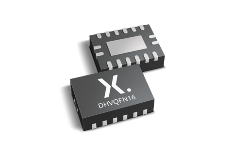
| 74CBTLV3253BQ | 2.3 - 3.6 | 3.3 | CMOS/LVTTL | 7 | 400 | 2 | 0.2 | very low | -40~125 | 93 | 13.7 | 62 | DHVQFN16 |
| 74CBTLV3253D | 2.3 - 3.6 | 3.3 | CMOS/LVTTL | 7 | 400 | 2 | 0.2 | very low | -40~125 | 92 | 9.6 | 52 | SO16 |
| 74CBTLV3253DS | 2.3 - 3.6 | 3.3 | CMOS/LVTTL | 7 | 400 | 2 | 0.2 | very low | -40~125 | 148 | 42 | 148 | SSOP16 |
| 74CBTLV3253PW | 2.3 - 3.6 | 3.3 | CMOS/LVTTL | 7 | 400 | 2 | 0.2 | very low | -40~125 | 125 | 4.4 | 54.6 | TSSOP16 |
Package
| Type number | Orderable part number, (Ordering code (12NC)) | Status | Marking | Package | Package information | Reflow-/Wave soldering | Packing |
|---|---|---|---|---|---|---|---|
| 74CBTLV3253BQ | 74CBTLV3253BQ,115 (935289997115) |
Active | TV3253 |

DHVQFN16 (SOT763-1) |
SOT763-1 | SOT763-1_115 | |
| 74CBTLV3253D | 74CBTLV3253D,118 (935289998118) |
Active | 74CBTLV3253D |

SO16 (SOT109-1) |
SOT109-1 |
SO-SOJ-REFLOW
SO-SOJ-WAVE WAVE_BG-BD-1 |
SOT109-1_118 |
| 74CBTLV3253DS | 74CBTLV3253DS,118 (935290001118) |
Active | TLV3253 |

SSOP16 (SOT519-1) |
SOT519-1 |
SSOP-TSSOP-VSO-REFLOW
SSOP-TSSOP-VSO-WAVE |
SOT519-1_118 |
| 74CBTLV3253PW | 74CBTLV3253PW,118 (935289999118) |
Active | TLV3253 |

TSSOP16 (SOT403-1) |
SOT403-1 |
SSOP-TSSOP-VSO-WAVE
|
SOT403-1_118 |
Environmental information
| Type number | Orderable part number | Chemical content | RoHS | RHF-indicator |
|---|---|---|---|---|
| 74CBTLV3253BQ | 74CBTLV3253BQ,115 | 74CBTLV3253BQ |
|
|
| 74CBTLV3253D | 74CBTLV3253D,118 | 74CBTLV3253D |
|
|
| 74CBTLV3253DS | 74CBTLV3253DS,118 | 74CBTLV3253DS |
|
|
| 74CBTLV3253PW | 74CBTLV3253PW,118 | 74CBTLV3253PW |
|
|
Documentation (20)
| File name | Title | Type | Date |
|---|---|---|---|
| 74CBTLV3253 | Dual 1-of-4 multiplexer/demultiplexer | Data sheet | 2024-04-23 |
| AN90063 | Questions about package outline drawings | Application note | 2026-06-17 |
| SOT763-1 | 3D model for products with SOT763-1 package | Design support | 2019-10-03 |
| SOT109-1 | 3D model for products with SOT109-1 package | Design support | 2020-01-22 |
| SOT519-1 | 3D model for products with SOT519-1 package | Design support | 2023-02-07 |
| SOT403-1 | 3D model for products with SOT403-1 package | Design support | 2020-01-22 |
| cbtlv3253 | cbtlv3253 IBIS model | IBIS model | 2013-04-08 |
| Nexperia_package_poster | Nexperia package poster | Leaflet | 2020-05-15 |
| DHVQFN16_SOT763-1_mk | plastic, dual in-line compatible thermal enhanced very thin quad flat package; 16 terminals; 0.5 mm pitch; 3.5 mm x 2.5 mm x 0.85 mm body | Marcom graphics | 2017-01-28 |
| SO16_SOT109-1_mk | plastic, small outline package; 16 leads; 1.27 mm pitch; 9.9 mm x 3.9 mm x 1.35 mm body | Marcom graphics | 2017-01-28 |
| TSSOP16_SOT403-1_mk | plastic, thin shrink small outline package; 16 leads; 0.65 mm pitch; 5 mm x 4.4 mm x 1.1 mm body | Marcom graphics | 2017-01-28 |
| SOT763-1 | plastic, leadless dual in-line compatible thermal enhanced very thin quad flat package; 16 terminals; 0.5 mm pitch; 3.5 mm x 2.5 mm x 1 mm body | Package information | 2023-05-11 |
| SOT109-1 | plastic, small outline package; 16 leads; 1.27 mm pitch; 9.9 mm x 3.9 mm x 1.75 mm body | Package information | 2023-11-07 |
| SOT519-1 | plastic, shrink small outline package; 16 leads; 0.635 mm pitch; 4.9 mm x 3.9 mm x 1.73 mm body | Package information | 2022-06-20 |
| SOT403-1 | plastic, thin shrink small outline package; 16 leads; 5 mm x 4.4 mm x 1.2 mm body | Package information | 2023-11-08 |
| SO-SOJ-REFLOW | Footprint for reflow soldering | Reflow soldering | 2009-10-08 |
| SSOP-TSSOP-VSO-REFLOW | Footprint for reflow soldering | Reflow soldering | 2009-10-08 |
| SO-SOJ-WAVE | Footprint for wave soldering | Wave soldering | 2009-10-08 |
| WAVE_BG-BD-1 | Wave soldering profile | Wave soldering | 2021-09-08 |
| SSOP-TSSOP-VSO-WAVE | Footprint for wave soldering | Wave soldering | 2009-10-08 |
Support
If you are in need of design/technical support, let us know and fill in the answer form we'll get back to you shortly.
Models
| File name | Title | Type | Date |
|---|---|---|---|
| SOT763-1 | 3D model for products with SOT763-1 package | Design support | 2019-10-03 |
| SOT109-1 | 3D model for products with SOT109-1 package | Design support | 2020-01-22 |
| SOT519-1 | 3D model for products with SOT519-1 package | Design support | 2023-02-07 |
| SOT403-1 | 3D model for products with SOT403-1 package | Design support | 2020-01-22 |
| cbtlv3253 | cbtlv3253 IBIS model | IBIS model | 2013-04-08 |
Ordering, pricing & availability
Sample
As a Nexperia customer you can order samples via our sales organization.
If you do not have a direct account with Nexperia our network of global and regional distributors is available and equipped to support you with Nexperia samples. Check out the list of official distributors.