


.png)
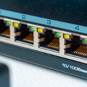
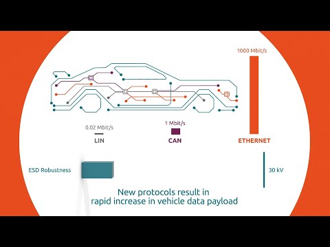
One major factor in the advancement of semiconductors has been shrinking structure geometries - allowing more functionality to be squeezed into smaller spaces. The downside is that complete systems, as well as individual ICs and data lines, become more sensitive to transient voltage pulses. Covering ESD protection and TVS devices as well as common-mode choke and EMI filtering, Nexperia's protection technologies have evolved with these trends - offering the highest level of protection in the industry's smallest packages, while minimizing any negative impact on signal integrity.
Featured products

Bipolar Discretes Q-portfolio
Nexperia introduces future-proof automotive portfolio for Bipolar Discretes ...

OPEN Alliance Ethernet ESD protection
Pioneering in automotive Ethernet OPEN Alliance compliant ESD protection
TrEOS protection for high speed data lines
Uncompromising TrEOS protection for sensitive high-speed interfaces.
Focus interfaces
Focus product families
Latest news and blogs
.6059742227349987662.jpg)


Latest videos


Parametric search
 Please wait, loading data...
Application note (2) |
|||
|---|---|---|---|
| File name | Title | Type | Date |
| AN90039_CN.pdf | 用于汽车以太网应用的ESD保护器件 100Base-T1、1000Base-T1) | Application note | 2023-04-18 |
| AN10753.pdf | ESD protection for USB 2.0 interfaces | Application note | 2021-04-14 |
Brochure (8) |
|||
| File name | Title | Type | Date |
| JPNexperia_ESD_Automotive_App_Guide.pdf | ESD Automotive Application Guide (JP) | Brochure | 2024-04-09 |
| Nexperia_ESD_Automotive_Application_Guide_CN.pdf | ESD保护 汽车 | Brochure | 2023-04-18 |
| Nexperia_ESD_Automotive_Application_Guide.pdf | ESD Automotive Application Guide | Brochure | 2023-02-16 |
| Nexperia_document_brochure_application-guide_automotive.pdf | Nexperia Application Guide Automotive | Brochure | 2019-05-31 |
| Nexperia_document_brochure_application-guide.pdf | Nexperia Application Guide | Brochure | 2019-05-31 |
| Nexperia_document_brochure_ESD-Protection-Applications_022017.pdf | ESD Protection Application guide | Brochure | 2018-12-21 |
| Application_Guide_for_ESD_protection_USB_3_2.pdf | Protected connection for mobile devices | Brochure | 2018-03-27 |
| Nexperia_document_brochure_IVN_protection_Factsheet.pdf | In-vehicle Network (IVN) ESD protection | Brochure | 2017-12-17 |
Leaflet (20) |
|||
| File name | Title | Type | Date |
| Final_Leaflet_1_V_ESD_portfolio.pdf | Final_Leaflet_1_V_ESD_portfolio | Leaflet | 2026-06-02 |
| Leaflet_CHN_Automotive_Ethernet_Leaflet.pdf | Leaflet_CHN_Automotive_Ethernet_Leaflet | Leaflet | 2025-02-19 |
| Leaflet_Automotive_Ethernet_FlipChip_LGA_Leaflet.pdf | Automotive Ethernet FlipChip LGA Leaflet | Leaflet | 2025-02-07 |
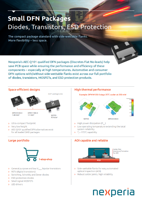
| nexperia_document_leaflet_DFN_Packages_Diodes_Transistors_ESD_Protection.pdf | DFN Packages Diodes Transistors ESD Protection | Leaflet | 2024-08-26 |
| Nexperia_Leaflet_Q-portfolio_car.pdf | Bipolar Discretes Q-portfolio | Leaflet | 2021-07-13 |
| ESD-Protection-for-automotive-infotainment-and-SerDes.pdf | ESD Protection for automotive infotainment and SerDes | Leaflet | 2021-04-19 |
| Compact-2-in-1-ESD-protection-for-high-speed-data-lines_CN.pdf | 高速数据线的 紧凑型二合一 TrEOS保护 | Leaflet | 2021-02-22 |
| Compact-2-in-1-TrEOS-protection-for-high-speed-data-lines.pdf | ESD Protection for HDMI USB and Thunderbolt in DFN0603-3 | Leaflet | 2021-02-01 |
| Nexperia_ESD_Protection_for_automotive_CAN-FD.pdf | ESD Protection for automotive CAN-FD | Leaflet | 2020-11-27 |
| ESD_protection_seminar_faq_document_japanese.pdf | ESD Protection Seminar FAQ Document Japanese | Leaflet | 2020-11-17 |
| ESD_proctection_seminar_q_a_document.pdf | ESD Protection Seminar Q & A Document | Leaflet | 2020-10-07 |
| Article_SEED_Round_Vehicle_Electronics.pdf | SEED modelling helps to develop automotive Ethernet ESD protection that meets Open Alliance specifications | Leaflet | 2020-09-28 |
| Nexperia_ESD_Protection_for_automotive_infotainment_and_SerDes_CN.pdf | ESD Protection for automotive infotainment and SerDes CN | Leaflet | 2020-07-15 |
| Nexperia_Integrated_CMF_and_ESD_protection_for_high-speed_data_lines_CN.pdf | Nexperia Integrated CMF and ESD protection for high-speed data lines CN | Leaflet | 2020-04-29 |
| Nexperia_CMF_with_ESD_protection_for_high-speed_datalines.pdf | CMF with ESD protection for high-speed data communication lines | Leaflet | 2020-04-03 |
| TrEOS_ESD_protection_for_USB_Type-C_leaflet_CN.pdf | 面向USB Type-C®的 | Leaflet | 2020-03-27 |
| Nexperia_TrEOS_ESD_protection_for_USB_Type-C_leaflet.pdf | TrEOS ESD protection for USB Type-C | Leaflet | 2020-03-06 |
| Nexperia_NFC_Antenna_Protection_diodes_leaflet.pdf | NFC Antenna Protection Diodes | Leaflet | 2019-05-31 |
| Nexperia_document_leaflet_PESD3V3V1BCSF-PESD3V3U1BCSF_UltraLowClamp_201805.pdf | Ultra low clamp 3.3 V reverse standoff voltage ESD protection | Leaflet | 2018-05-08 |
| Nexperia_document_leaflet_MobileTVS_201804.pdf | TVS for Mobile applications | Leaflet | 2018-05-08 |
Marcom graphics (1) |
|||
| File name | Title | Type | Date |
| DFN1006-2_SOD882_mk.png | plastic, leadless ultra small package; 2 terminals; 0,65 mm pitch; 1 mm x 0.6 mm x 0.48 mm body | Marcom graphics | 2017-01-28 |
Selection guide (1) |
|||
| File name | Title | Type | Date |
| nexperia_automotive_selection_guide_LR_201902.pdf | Nexperia Automotive Selection Guide 2019 | Selection guide | 2019-02-18 |
User manual (1) |
|||
| File name | Title | Type | Date |
| nexperia_ESD_Handbook_230720_lowres.pdf | nexperia_ESD_Handbook_230720_lowres | User manual | 2023-05-30 |
White paper (12) |
|||
| File name | Title | Type | Date |
| Final_Whitepaper_Best_practices_to_protect_USB4_NEX_Kandou.pdf | Whitepaper_Best_practices_to_protect_USB4_NEX_Kandou | White paper | 2026-06-02 |
| FINAL_2025-0001-NEX_134_Whitepaper-ESD-for-USB.pdf | Why ESD Diode Placement Matters: Optimizing Protection for AC-Coupled SuperSpeed Data Lines | White paper | 2025-08-06 |
| Nexperia_White_paper_Using_ESD_Protection_Device_as_a_3D_Model_in_Simulations_082024.pdf | ESD protection devices in 3D Model Simulations. | White paper | 2024-05-31 |
| Nexperia_Whitepaper_ESD_Protection_for_Automotive_GER.pdf | ESD-Schutz für High-Speed-Video-Links im Automobil | White paper | 2021-11-16 |
| Nexperia_Whitepaper_ESD_Protection_for_Automotive_High-Speed_Video_Links_CN.pdf | 汽车高速视频链路的ESD保护 | White paper | 2021-08-06 |
| Nexperia_Whitepaper_ESD_Protection_for_Automotive_High-Speed_Video_Links.pdf | ESD Protection for Automotive High-Speed Video Links | White paper | 2021-07-13 |
| Whitepaper_ESD_protection_devices_for_USB4_CN.pdf | 为USB4TM选择ESD保护器件 | White paper | 2020-03-27 |
| Whitepaper_ESD_protection_devices_for_USB4.pdf | Choosing ESD protection devices for USB4 | White paper | 2020-03-06 |
| Nexperia_Whitepaper_ESD_Discharge_Current_Measurement_Using_SEED_CN.pdf | 运用SEED设计方法,根据开放技术联盟100BASE-T1规范 | White paper | 2020-02-26 |
| WhitePaper_TVS_Diodes.pdf | What are TVS diodes and how do you choose the right one? | White paper | 2020-02-12 |
| WhitePaper-protecting-super-speed-interfaces-against-EMI.pdf | Whitepaper: Effectively protecting super-speed interfaces against EMI | White paper | 2020-01-29 |
| Nexperia_Whitepaper_ESD_Discharge_Current_Measurement_Using_SEED_1.pdf | Efficient prediction of ESD discharge current according to OPEN Alliance 100BASE-T1 specification using SEED | White paper | 2019-12-19 |
Please contact us if you have any questions. If you are in need of design support, please fill in the technical support form, we will get back to you shortly.
Please visit our engineer exchange forum or contact us for further support.
Frequently Asked Questions
At Nexperia we focus on device modelling including SPICE models. However, we do not use SPICE models considering air gaps due to poor repeatability of results. Models with contact discharge and optimized signal integrity show better measurement quality. For even better insights, we recommend to use SEED simulation representing the application and ESD event very precisely.
The maximum resistance is always given by the application. You should try without additional resistance in the beginning. If you see that you cannot reach the target ESD level, you have to evaluate how much the application allows you to add and, try if this is sufficient.
Throughout history, new ESD protection technologies were developed. First, people used large capacitors, but they have extremely bad clamping behaviour and are not applicable for data lines. Next, Zener diodes were used and optimized. This can be applied to both internal IC as well as external ESD protection. The main target is to reduce the clamping voltage to lower the ESD stress within the IC and system. New approaches such as "snap-back" behaviour offer a great protection behaviour to lower the clamping voltage. In addition, new materials and structures can be considered and help to improve the device level robustness for assembly but also the more important system level robustness.
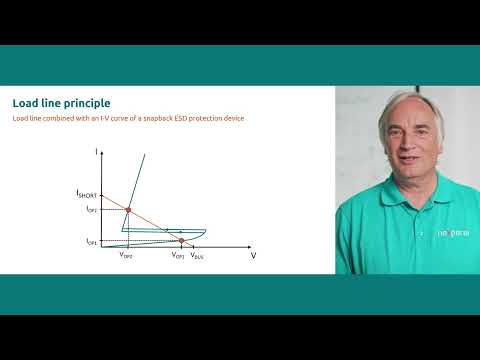
The clamping voltage can be lower than breakdown voltage due to protection behaviours where the clamping voltage is actively lowered. The "snap-back" technology is a great example. A lower clamping voltage offers better system level protection and is not a disadvantage.
The gradient of the tangent in the operating point (OP) provides the dynamic resistance Rdyn (TLP). Rdyn (TLP) is determined for reverse and forward directions of the DUT. In fact of the linear behaviour V = f(I), the tangent in the operating point can be approximated via the trendline Linear VCL (TLP) = f(I) and hence provides the dynamic resistance Rdyn (TLP).
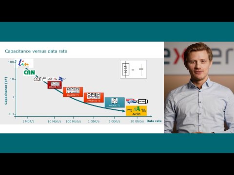
The relative deviation of capacitance of separate ESD protection devices is almost the same. For instance, a 20 pF device for CAN bus shows about the same relative capacitance deviation as a 2 pF solution for Ethernet protection. As such, the absolute capacitance deviation becomes smaller if the device capacitance is lower. In this case, a 2 pF solution would show only 0.2 pF deviation (10% relative) showing minor impact on signal integrity and performance.
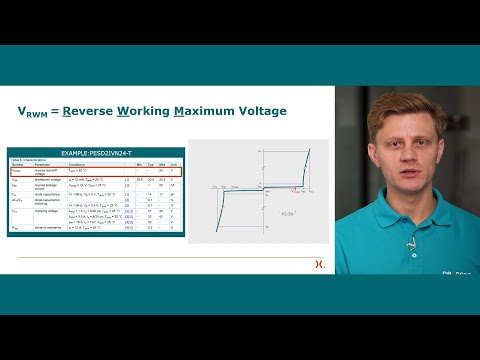
The reverse working maximum voltage VRWM indicates the DC voltage that can be applied without the device being active in order to not interrupt normal operation mode. The breakdown voltage VBR is higher compared to the VRWM and describes the transition of non-operating to operating mode. This can be also seen at the stated current. Therefore, there is a gap between both voltages to ensure safe operation.
On the shown PCB, the ground connection is on the upper left. Thus, in case of the ESD event with external ESD protection, the current flows through the protection device directly to ground as the ESD protection functions as a current divider. Without external ESD protection, the ESD pulse can flow directly through the traces into the IC causing malfunction and less current flows to ground.
Power dissipation is the product of clamping voltage times peak pulse current: P = U x I. For instance, IPP = 5 A and VCL = 41 V would result in 205 W. Important to mention is that you can only draw limited information about the robustness and do not learn about the system level robustness. In case of a "snap-back" protection behaviour where the clamping voltage is actively lowered, the power dissipation would be lower as well. This can be confusing since the "snap-back" behaviour offers superior ESD protection. Therefore, the power dissipation does not provide a good indication of ESD robustness.
Basically, everything can be destroyed but it is difficult to detect the exact root cause once the device is fully destroyed. To reconstruct the failure mode, a disruptive physical analysis and further investigation including SEED simulation can help.
The parameters clamping voltage and peak pulse current provide a good indication of ESD protection. A low clamping voltage will, in effect, lower the shoulder of the ESD waveform. Different ESD protection technologies such as open-base transistors or thyristors with a "snap-back" behaviour can improve further.
SEED (System Efficient ESD Design) simulation is an effective approach to simulate an ESD event. It especially helps to match an IC with discrete ESD protection. For further introduction, we recommend our white paper describing the concept and basic steps.
An EMI scanner can be used to measure the magnetic field and current flow on the PCB in case of ESD event. It operates with a near field probe which is positioned above the circuit. The duration ESD Event is roughly 100 ns. The EMI scanner cannot simulate but records a video of the PCB under test. The blue colour indicates low current density where the yellow or red colour indicates high current density. As such, it is possible to get a visual insight of ESD concept effectivity.
Temperature is a major factor for derating parameters, however, silicon based ESD protection is characterized by minor performance loss over temperature. Thermal robustness is usually provided in the datasheet for a typical PCB stackup.
The main difference is the topology. The snap back devices have the open base or silicon controlled rectifier topology. Both of them allow to snap back which results in significant clamping voltage reduction. In comparison, a Zener protection starts to clamp when the breakdown voltage is achieved and clamping voltage is increasing slowly. All typologies should be considered when choosing an ESD protection device, though, for high-speed lines a snap-back typology will increase performance significantly.
It is possible to stack ESD protection devices in series. If you place two times the same ESD protection in series, the following happens:
- VRWM is doubled
- Trigger / breakdown is doubled
- Vclamping is doubled
- CD is halved
Nexperia offers consultancy and evaluation support on customer request. Extra cost may arise on an individual basis for e.g. special test boards. Please reach out to your Nexperia contact for further details.
Usually, the ESD protection devices survive a reasonable amount of ESD pulses very well, without degradation. Thermal issues should be considered when a longer duration surge pulses are applied.
If a snap-back device is triggered, a latch-up can happen if the on-state current is higher than the hold current of the ESD protection device. However, most ESD protection devices withstand the current arising from this condition: Nexperia parts were tested in latch-up with 100mA for several hours without showing any damage or degradation. If an interface is affected, a soft fail occurs but no hardware fail. For many interfaces, the snap-back device automatically returns to its off-state once the affected data line is in single-ended low state.
Nexperia uses industry proven mold compounds that fulfil all automotive quality requirements such as AEC-Q101 or MSL levels. Damage caused by electrical overstress (EOS) can be prevented by application design. In addition, a high IPPM value can increase safety margin on device level.
ESD protection devices are usually robust devices. However, the environmental impacts usually are covered by qualifications tests, such as AEC-Q101 or similar.
Usually, the forward voltage of ESD protection devices is not of importance for ESD purposes. However, this information can be shared with you on demand.
While applying repeating spikes the device might be heated up. The increasing temperature will for sure impact the electrical behaviour, such as the break down voltage. We provide a measurement data over temperature on demand.
The cross talk of ESD events is strongly dependent on your sub-application including the PCB, its stack-up etc. So, we cannot give a specific recommendation.
The IC are typically robust for HBM up to 2kV. Or at least 500V. In addition, this is the first peak with has a duration of a few nanoseconds only. There is not much energy in this strike, and hence, usually not a problem for classic networks. It can be a problem for very sensitive, e.g. high speed ICs. Therefore, we suggest to use ESD devices with very low trigger and clamping voltage and, in addition with smallest parasitics, e.g. leadless packages, as discussed during the second session.
Quality requirements from customers may deviate due to individual assembly guidelines and special quality aspects. Nexperia offers dedicated product groups to fulfil highest quality standards above AEC-Q101.
The ESD protection should always be placed close to the connector in order to work as current divider and clamp the ESD current to ground. Depending on board net voltage, a higher VBR must be considered. For instance, for a 24 V board net, a VBR of >32 V should be chosen.
The trigger voltage is more determined by the physical structure of the ESD device but the dynamic resistance has a minor impact on the triggering behaviour as well.
Nexperia provides a parametric search to filter certain parameters on our webpage.
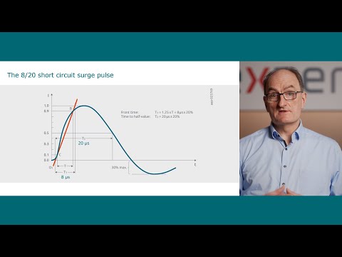
The transmission line pulse (TLP) is a short-duration rectangular pulse in a controlled impedance environment of 50Ω, which improves test accuracy and measurement reproducibility.
TLP characterizes performance attributes of devices under stresses that have a short pulse width and fast rise time. Each measurement result becomes a point on the TLP graph that shows a TLP I-V characteristic, i.e. the TLP-curve.
Nexperia automotive grades products are AEC-Q101 qualified if indicated in the datasheet. The ESD devices show very low self-heating since no power is applied. In addition, Nexperia performs several reliability tests according to JEDEC and ISO norms to ensure high reliability.
Basically, there a two ESD failure modes: destructive where the device is damaged and non-destructive which show soft failure. Non-destructive failures are hard to detect but it helps to perform tests under incrementally higher voltages to determine destructive failure point. As such, sometimes degradation of the device can be detected early which provides a first indication of potential risk. Deviation of leakage current gives also a good indication.
For 24 V DC power line, a reverse standoff voltage of min. 32 V is required due to jump start requirements
SEED (System Efficient ESD Design) simulation is an effective approach to simulate an ESD event. It especially helps to match an IC with discrete ESD protection. For further introduction, we recommend our white paper describing the concept and basic steps
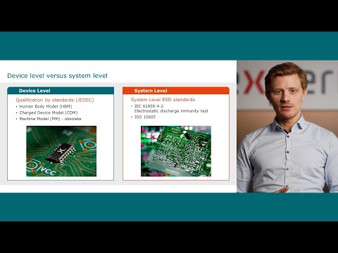
The ESD design strategy is independent due to general ESD design aspects. However, additional requirements may narrow the range of suitable protection devices and include further tests. For instance, the ISO10605 states additional tests for automotive applications.
Nexperia automotive grades products are AEC-Q101 qualified if indicated in the datasheet. All of our products are considered basic building blocks, where the functional safety criticality is defined by the system. This is important as a default failure mode for one device/system may not be suitable for another, and is the reason why we cannot assume any ASIL rating based on the ISO26262 methodology. Nexperia can provide further details and support to customers who will use ESD protection devices in safety critical applications.
Scattering parameters can be included in datasheets depending on application and protection device. S-Parameter data can be send via e-mail on demand.
For sub GHz applications, the ESD protection device capacitance shows major impact on impedance. To improve impedance curve, a lower capacitance device may improve performance. The package has a minor impact in this area.
Cross talk depends on the sub-system. As PCB designs become smaller and show a higher density of traces, there might be a higher risk of cross talk. However, this is more on the PCB surface and not the periphery.
If using just a capacitor, the ESD pulse might be damped a little but the system level protection is very low. A discrete ESD protection device adds significant improvement of system level ESD robustness and increase system reliability.
The conducted discharge on the connector is only minor impacted by the housing of the module you are designing. The air discharge is very strongly depending the housing and, hence, should be considered during development.
For DFN package soldering and AOI guidelines, please refer to Nexperia application notes.
In this example with PCB having 4 or more layers, the GND layer is just below the top layer with a prepreg of around 100 µm. So the via inductance of 100µm is small. However, depending on your PCB stack up you may route your GND pin differently.
Coax (single ended) or differential transmission has not a real impact on the electrical performance of the ESD protection device. It might impact the package of your protections device, since you need to decide how many lines you have to protect.
We are currently working on eye diagram measurements and simulations for other applications besides USBx and HDMIx.
A TLP curve comparison provides a quick indication for this. As such, the ESD protection device should trigger before the internal ESD protection of the PHY. For instance, a good match would be if the breakdown voltage of the ESD protection is 35 V and the breakdown voltage of the PHY is 60 V. In this combination, the ESD protection clamps first and takes the vast majority of ESD pulse.
There might be some issues related to DPI test. Those are, when too much energy is getting absorbed by the network during the test. In such case you need to choose a ESD protection device with higher trigger voltage.
The traces should be routed directly to the ESD protection device without changing layer or coupling to other PCB structure. However, the routing depends strongly on the sub-application and cannot be covered in datasheets.
All Nexperia packages fulfil AEC-Q101 and other, highest quality standards.
The reason is the during the DPI test RF noise can achieve amplitudes up to 100 V. To avoid clamping of the ESD protection device, the triggering voltage was defined to be >100 V. The DC voltage over 24 V is related to the short to battery requirement (similar as for CAN/LIN).
For some application such as LIN/CAN/Ethernet the 3-pin package does not impact the signal integrity significantly. For high frequency applications such as SerDes and Multimedia we recommend other, e.g. leadless packages.
For 1000BASE-T1 the PESD2ETH1G-T can be used with even smaller parasitic capacitance (<2 pF). For further product information use the selection guide on the webpage.
By an eye diagram you can judge if the ESD protection is impacting your digital system too much or not. Besides S-parameters and parasitic capacitance, this is another view on the signal integrity on device level.
For CAN it is more importance to look on the capacitance. However, for some CAN products Nexperia also provides S-parameters for CAN products.
For further product information please visit our webpage