


74CB3Q3253
Dual 1-of-4 FET multiplexer/demultiplexer with charge pump
The 74CB3Q3253 is a dual high-bandwidth single-pole, quad-throw FET bus switch. Each switch features a select input (Sn) and an output enable input (nOE). The switch is disabled when the nOE input is HIGH. An internal charge-pump increases the gate voltage of the NMOS pass transistor. The result is improved RON and RON(flat) performance and the ability to switch 5 V signals when VCC = 3.3 V.
Features and benefits
Wide supply voltage range from 2.3 V to 3.6 V
Overvoltage switching on switch ports:
0 V to 5 V switching with VCC = 2.5 V
0 V to 5 V switching with VCC = 3.3 V
Switch voltage accepts signals up to 5.5 V
4 Ω (typical) ON resistance
3.5 pF (typical) OFF-state capacitance
High bandwidth 0.5 GHz (maximum)
Low input/output capacitance minimizes loading and signal distortion
Fast switching frequency fmax = 20 MHz (maximum)
Low power consumption ICC = 0.4 mA (typical)
Control inputs can be driven by TTL or 5 V/3.3 V CMOS outputs
IOFF supports partial power-down mode operation
Latch-up performance exceeds 100 mA per JESD 78E Class II Level A
ESD protection:
HBM: ANSI/ESDA/JEDEC JS-001 class 2 exceeds 2000 V
CDM: ANSI/ESDA/JEDEC JS-002 class C3 exceeds 1000 V
Specified from -40 °C to +85 °C
Applications
Communication infrastructure
Bus isolation
Memory interleaving
Sensor multiplexing
Parametrics
| Type number | VCC (V) | VPASS (V) | Logic switching levels | RON (Ω) | Nr of bits | tpd (ns) | Power dissipation considerations | Tamb (°C) | Rth(j-a) (K/W) | Ψth(j-top) (K/W) | Rth(j-c) (K/W) | Package name | |
|---|---|---|---|---|---|---|---|---|---|---|---|---|---|
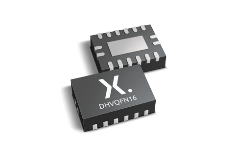
| 74CB3Q3253BQ | 2.3 - 3.6 | Vcc | CMOS/LVTTL | 4 | 2 | 0.2 | very low | -40~85 | 84 | 7.3 | 51.5 | DHVQFN16 | |
| 74CB3Q3253PW | 2.3 - 3.6 | Vcc | CMOS/LVTTL | 4 | - | 2 | 0.2 | very low | -40~85 | 116 | 2.4 | 44.3 | TSSOP16 |
Package
| Type number | Orderable part number, (Ordering code (12NC)) | Status | Marking | Package | Package information | Reflow-/Wave soldering | Packing |
|---|---|---|---|---|---|---|---|
| 74CB3Q3253BQ | 74CB3Q3253BQX (935339208115) |
Active | 3Q3253 |
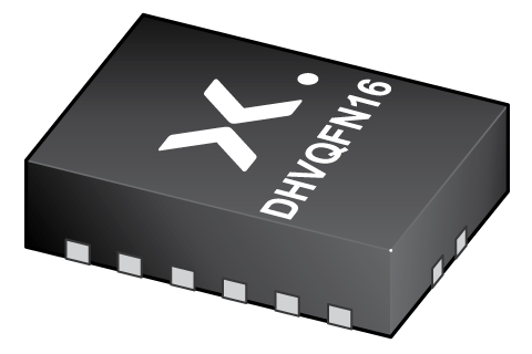
DHVQFN16 (SOT763-1) |
SOT763-1 | SOT763-1_115 | |
| 74CB3Q3253PW | 74CB3Q3253PWJ (935339209118) |
Active | B3Q3253 |
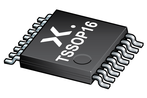
TSSOP16 (SOT403-1) |
SOT403-1 |
SSOP-TSSOP-VSO-WAVE
|
SOT403-1_118 |
Environmental information
| Type number | Orderable part number | Chemical content | RoHS | RHF-indicator |
|---|---|---|---|---|
| 74CB3Q3253BQ | 74CB3Q3253BQX | 74CB3Q3253BQ |
|
|
| 74CB3Q3253PW | 74CB3Q3253PWJ | 74CB3Q3253PW |
|
|
Documentation (11)
| File name | Title | Type | Date |
|---|---|---|---|
| 74CB3Q3253 | Dual 1-of-4 FET multiplexer/demultiplexer with charge pump | Data sheet | 2024-04-11 |
| AN90063 | Questions about package outline drawings | Application note | 2025-10-22 |
| SOT763-1 | 3D model for products with SOT763-1 package | Design support | 2019-10-03 |
| SOT403-1 | 3D model for products with SOT403-1 package | Design support | 2020-01-22 |
| Nexperia_document_leaflet_CB3Q_switches_201803 | CB3Q Bus Switches | Leaflet | 2018-04-06 |
| Nexperia_package_poster | Nexperia package poster | Leaflet | 2020-05-15 |
| DHVQFN16_SOT763-1_mk | plastic, dual in-line compatible thermal enhanced very thin quad flat package; 16 terminals; 0.5 mm pitch; 3.5 mm x 2.5 mm x 0.85 mm body | Marcom graphics | 2017-01-28 |
| TSSOP16_SOT403-1_mk | plastic, thin shrink small outline package; 16 leads; 0.65 mm pitch; 5 mm x 4.4 mm x 1.1 mm body | Marcom graphics | 2017-01-28 |
| SOT763-1 | plastic, leadless dual in-line compatible thermal enhanced very thin quad flat package; 16 terminals; 0.5 mm pitch; 3.5 mm x 2.5 mm x 1 mm body | Package information | 2023-05-11 |
| SOT403-1 | plastic, thin shrink small outline package; 16 leads; 5 mm x 4.4 mm x 1.2 mm body | Package information | 2023-11-08 |
| SSOP-TSSOP-VSO-WAVE | Footprint for wave soldering | Wave soldering | 2009-10-08 |
Support
If you are in need of design/technical support, let us know and fill in the answer form we'll get back to you shortly.
Ordering, pricing & availability
Sample
As a Nexperia customer you can order samples via our sales organization.
If you do not have a direct account with Nexperia our network of global and regional distributors is available and equipped to support you with Nexperia samples. Check out the list of official distributors.