


74HC109-Q100; 74HCT109-Q100
Dual JK flip-flop with set and reset; positive-edge-trigger
The 74HC109-Q100; 74HCT109-Q100 is a dual positive edge triggered JK flip-flop featuring individual J and K inputs, clock (CP) inputs, set (SD) and reset (RD) inputs and complementary Q and Q outputs. The set and reset are asynchronous active LOW inputs and operate independently of the clock input. The J and K inputs control the state changes of the flip-flops as described in the mode select function table. The J and K inputs must be stable one set-up time prior to the LOW-to-HIGH clock transition for predictable operation. The JK design allows operation as a D-type flip-flop by connecting the J and K inputs together. This device features reduced input threshold levels to allow interfacing to TTL logic levels. Inputs also include clamp diodes, this enables the use of current limiting resistors to interface inputs to voltages in excess of VCC.
Schmitt-trigger action in the clock input makes the circuit highly tolerant to slower clock rise and fall times.
This product has been qualified to the Automotive Electronics Council (AEC) standard Q100 (Grade 1) and is suitable for use in automotive applications.
Features and benefits
Automotive product qualification in accordance with AEC-Q100 (Grade 1)
Specified from -40 °C to +85 °C and from -40 °C to +125 °C
J and K inputs for easy D-type flip-flop
Toggle flip-flop or "do nothing" mode
Wide supply voltage range:
For 74HC109-Q100: from 2.0 V to 6.0 V
For 74HCT109-Q100: from 4.5 V to 5.5 V
CMOS low power dissipation
High noise immunity
Input levels:
For 74HC109-Q100: CMOS level
For 74HCT109-Q100: TTL level
Latch-up performance exceeds 100 mA per JESD 78 Class II Level B
74HC109-Q100 complies with JEDEC standards:
JESD8C (2.7 V to 3.6 V)
JESD7A (2.0 V to 6.0 V)
74HCT109-Q100 complies with JEDEC standard JESD7A (2.0 V to 6.0 V)
ESD protection:
HBM: ANSI/ESDA/JEDEC JS-001 class 2 exceeds 2000 V
CDM: ANSI/ESDA/JEDEC JS-002 class C3 exceeds 1000 V
Parametrics
| Type number | VCC (V) | Logic switching levels | Output drive capability (mA) | tpd (ns) | fmax (MHz) | Power dissipation considerations | Tamb (°C) | Rth(j-a) (K/W) | Ψth(j-top) (K/W) | Rth(j-c) (K/W) | Package name |
|---|---|---|---|---|---|---|---|---|---|---|---|
| 74HC109D-Q100 | 2.0 - 6.0 | CMOS | ± 5.2 | 15 | 75 | low | -40~125 | 86 | 6.6 | 44 | SO16 |
| 74HCT109D-Q100 | 4.5 - 5.5 | TTL | ± 4 | 17 | 61 | low | -40~125 | 86 | 6.6 | 44 | SO16 |
| 74HCT109PW-Q100 | 4.5 - 5.5 | TTL | ± 4 | 17 | 61 | low | -40~125 | 119 | 3.2 | 48.1 | TSSOP16 |
Package
| Type number | Orderable part number, (Ordering code (12NC)) | Status | Marking | Package | Package information | Reflow-/Wave soldering | Packing |
|---|---|---|---|---|---|---|---|
| 74HC109D-Q100 | 74HC109D‑Q100J (935334221118) |
Active | 74HC109D |
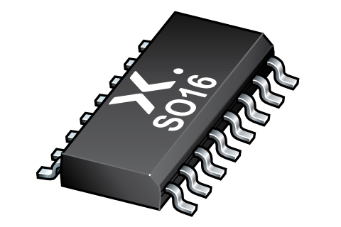
SO16 (SOT109-1) |
SOT109-1 |
SO-SOJ-REFLOW
SO-SOJ-WAVE WAVE_BG-BD-1 |
SOT109-1_118 |
| 74HCT109D-Q100 | 74HCT109D‑Q100J (935332777118) |
Active | 74HCT109D |
SO16 (SOT109-1) |
SOT109-1 |
SO-SOJ-REFLOW
SO-SOJ-WAVE WAVE_BG-BD-1 |
SOT109-1_118 |
| 74HCT109PW-Q100 | 74HCT109PW‑Q100J (935336488118) |
Active | HCT109 |
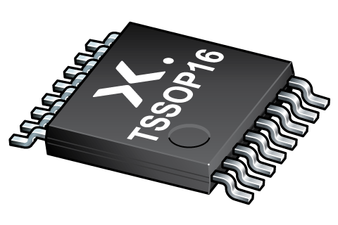
TSSOP16 (SOT403-1) |
SOT403-1 |
SSOP-TSSOP-VSO-WAVE
|
SOT403-1_118 |
Environmental information
| Type number | Orderable part number | Chemical content | RoHS | RHF-indicator |
|---|---|---|---|---|
| 74HC109D-Q100 | 74HC109D‑Q100J | 74HC109D-Q100 |
|
|
| 74HCT109D-Q100 | 74HCT109D‑Q100J | 74HCT109D-Q100 |
|
|
| 74HCT109PW-Q100 | 74HCT109PW‑Q100J | 74HCT109PW-Q100 |
|
|
Documentation (15)
| File name | Title | Type | Date |
|---|---|---|---|
| 74HC_HCT109_Q100 | Dual JK flip-flop with set and reset; positive-edge-trigger | Data sheet | 2024-02-21 |
| AN11044 | Pin FMEA 74HC/74HCT family | Application note | 2019-01-09 |
| AN90063 | Questions about package outline drawings | Application note | 2025-10-22 |
| SOT109-1 | 3D model for products with SOT109-1 package | Design support | 2020-01-22 |
| SOT403-1 | 3D model for products with SOT403-1 package | Design support | 2020-01-22 |
| Nexperia_package_poster | Nexperia package poster | Leaflet | 2020-05-15 |
| SO16_SOT109-1_mk | plastic, small outline package; 16 leads; 1.27 mm pitch; 9.9 mm x 3.9 mm x 1.35 mm body | Marcom graphics | 2017-01-28 |
| TSSOP16_SOT403-1_mk | plastic, thin shrink small outline package; 16 leads; 0.65 mm pitch; 5 mm x 4.4 mm x 1.1 mm body | Marcom graphics | 2017-01-28 |
| SOT109-1 | plastic, small outline package; 16 leads; 1.27 mm pitch; 9.9 mm x 3.9 mm x 1.75 mm body | Package information | 2023-11-07 |
| SOT403-1 | plastic, thin shrink small outline package; 16 leads; 5 mm x 4.4 mm x 1.2 mm body | Package information | 2023-11-08 |
| SO-SOJ-REFLOW | Footprint for reflow soldering | Reflow soldering | 2009-10-08 |
| HCT_USER_GUIDE | HC/T User Guide | User manual | 1997-10-31 |
| SO-SOJ-WAVE | Footprint for wave soldering | Wave soldering | 2009-10-08 |
| WAVE_BG-BD-1 | Wave soldering profile | Wave soldering | 2021-09-08 |
| SSOP-TSSOP-VSO-WAVE | Footprint for wave soldering | Wave soldering | 2009-10-08 |
Support
If you are in need of design/technical support, let us know and fill in the answer form we'll get back to you shortly.
Ordering, pricing & availability
Sample
As a Nexperia customer you can order samples via our sales organization.
If you do not have a direct account with Nexperia our network of global and regional distributors is available and equipped to support you with Nexperia samples. Check out the list of official distributors.