


74LVC16374A-Q100; 74LVCH16374A-Q100
16-bit edge-triggered D-type flip-flop; 5 V tolerant; 3-state
The 74LVC16374A-Q100; 74LVCH16374A-Q100 is a 16-bit edge-triggered D-type flip-flop with 3-state outputs. The device can be used as two 8-bit flip-flops or one 16-bit flip-flop. The device features two clocks (1CP and 2CP) and two output enables (1OE and 2OE), each controlling 8-bits. The flip-flops will store the state of their individual D-inputs that meet the set-up and hold time requirements on the LOW-to-HIGH clock (nCP) transition. A HIGH on nOE causes the outputs to assume a high-impedance OFF-state. Operation of the nOE input does not affect the state of the flip-flops . Inputs can be driven from either 3.3 V or 5 V devices. This feature allows the use of these devices as translators in mixed 3.3 V and 5 V environments.
Schmitt-trigger action at all inputs makes the circuit tolerant of slower input rise and fall times.
This device is fully specified for partial power down applications using IOFF. The IOFF circuitry disables the output, preventing the potentially damaging backflow current through the device when it is powered down.
This product has been qualified to the Automotive Electronics Council (AEC) standard Q100 (Grade 1) and is suitable for use in automotive applications.
Features and benefits
Automotive product qualification in accordance with AEC-Q100 (Grade 1)
Specified from -40 °C to +85 °C and from -40 °C to +125 °C
Overvoltage tolerant inputs to 5.5 V
Wide supply voltage range from 1.2 V to 3.6 V
CMOS low power dissipation
Multibyte flow-through standard pinout architecture
Low inductance multiple supply pins for minimum noise and ground bounce
Direct interface with TTL levels
All data inputs have bus hold (74LVCH16374A-Q100 only)
High-impedance outputs when VCC = 0 V
Complies with JEDEC standard:
JESD8-7A (1.65 V to 1.95 V)
JESD8-5A (2.3 V to 2.7 V)
JESD8-C/JESD36 (2.7 V to 3.6 V)
ESD protection:
HBM: ANSI/ESDA/JEDEC JS-001 class 2 exceeds 2000 V
CDM: ANSI/ESDA/JEDEC JS-002 class C3 exceeds 1000 V
Parametrics
| Type number | VCC (V) | Logic switching levels | Output drive capability (mA) | tpd (ns) | fmax (MHz) | Power dissipation considerations | Tamb (°C) | Rth(j-a) (K/W) | Ψth(j-top) (K/W) | Rth(j-c) (K/W) | Package name |
|---|---|---|---|---|---|---|---|---|---|---|---|
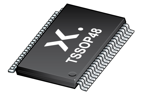
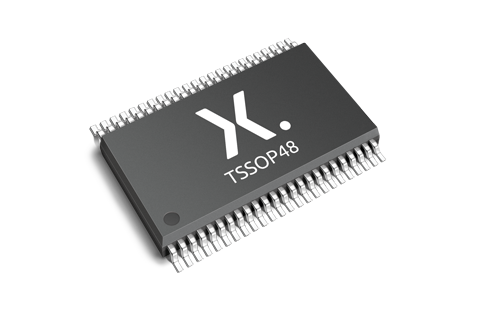
| 74LVC16374ADGG-Q100 | 1.2 - 3.6 | CMOS/LVTTL | ± 24 | 3.8 | 150 | low | -40~125 | 82 | 2 | 37 | TSSOP48 |
| 74LVCH16374ADGG-Q100 | 1.2 - 3.6 | CMOS/LVTTL | ± 24 | 3.8 | 150 | low | -40~125 | 82 | 2 | 37 | TSSOP48 |
Package
| Type number | Orderable part number, (Ordering code (12NC)) | Status | Marking | Package | Package information | Reflow-/Wave soldering | Packing |
|---|---|---|---|---|---|---|---|
| 74LVC16374ADGG-Q100 | 74LVC16374ADGG‑Q1J (935300232118) |
Active | LVC16374A |
TSSOP48 (SOT362-1) |
SOT362-1 |
SSOP-TSSOP-VSO-WAVE
|
SOT362-1_118 |
| 74LVCH16374ADGG-Q100 | 74LVCH16374ADGG‑QJ (935300357118) |
Active | LVCH16374A |
TSSOP48 (SOT362-1) |
SOT362-1 |
SSOP-TSSOP-VSO-WAVE
|
SOT362-1_118 |
Environmental information
| Type number | Orderable part number | Chemical content | RoHS | RHF-indicator |
|---|---|---|---|---|
| 74LVC16374ADGG-Q100 | 74LVC16374ADGG‑Q1J | 74LVC16374ADGG-Q100 |
|
|
| 74LVCH16374ADGG-Q100 | 74LVCH16374ADGG‑QJ | 74LVCH16374ADGG-Q100 |
|
|
Documentation (11)
| File name | Title | Type | Date |
|---|---|---|---|
| 74LVC_LVCH16374A_Q100 | 16-bit edge-triggered D-type flip-flop; 5 V tolerant; 3-state | Data sheet | 2024-04-22 |
| AN11009 | Pin FMEA for LVC family | Application note | 2019-01-09 |
| AN263 | Power considerations when using CMOS and BiCMOS logic devices | Application note | 2023-02-07 |
| AN90063 | Questions about package outline drawings | Application note | 2025-10-22 |
| SOT362-1 | 3D model for products with SOT362-1 package | Design support | 2020-01-22 |
| lvc16374a | lvc16374a IBIS model | IBIS model | 2013-04-08 |
| lvch16374a | lvch16374a IBIS model | IBIS model | 2013-04-09 |
| Nexperia_package_poster | Nexperia package poster | Leaflet | 2020-05-15 |
| TSSOP48_SOT362-1_mk | plastic, thin shrink small outline package; 48 leads; 0.5 mm pitch; 12.8 mm x 6.1 mm x 1.2 mm body | Marcom graphics | 2017-01-28 |
| SOT362-1 | plastic thin shrink small outline package; 48 leads; body width 6.1 mm | Package information | 2024-01-05 |
| SSOP-TSSOP-VSO-WAVE | Footprint for wave soldering | Wave soldering | 2009-10-08 |
Support
If you are in need of design/technical support, let us know and fill in the answer form we'll get back to you shortly.
Models
| File name | Title | Type | Date |
|---|---|---|---|
| SOT362-1 | 3D model for products with SOT362-1 package | Design support | 2020-01-22 |
| lvc16374a | lvc16374a IBIS model | IBIS model | 2013-04-08 |
| lvch16374a | lvch16374a IBIS model | IBIS model | 2013-04-09 |
Ordering, pricing & availability
Sample
As a Nexperia customer you can order samples via our sales organization.
If you do not have a direct account with Nexperia our network of global and regional distributors is available and equipped to support you with Nexperia samples. Check out the list of official distributors.