


NPS1000
0.5 V to 1.0 V, 1.5 A peak, 11 mΩ, load switch
NPS1000 is a low voltage, single-channel load switch with a low RDS,ON (11 mΩ) to minimize IR drop and power loss. It supports up to 0.6 A RMS current and a peak current of 1.5 A.
The switch is controlled by an EN input which is compatible with 1.2 V logic levels. When the load switch is enabled, the internal switch charges the output capacitor with a controlled inrush current. When the switch is disabled, an 8 Ω on-chip resistor discharges the output to ground and keeps it from floating.
The IC is powered from a separate BIAS pin which is rated for 2.3 V to 5.0 V operation.
NPS1000 has an over-temperature protection that latches the device OFF when the internal junction temperature is above the set point (Tth(OTLO)). At this time, the internal switch is turned off and the output discharge element turns on to discharge the output capacitor. The load switch can be enabled again by toggling the EN pin.
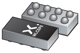
NPS1000 is available in an ultra-small, space saving, wafer level chip-scale package; 8 bumps; 1.42 mm × 0.72 mm × 0.465 mm body and is characterized for operation over junction temperature range of –40 °C to 105 °C.
 |
Features and benefits
- 0.5 V – 1.0 V operation voltage
- Low RDS,ON: 11 mΩ typical at 25 °C, 16 mΩ (maximum) at 85 °C
- Enable logic supports 1.2 V logic levels
- 0.6 A RMS and 1.5 A peak current capability
- Controlled start-up
- <200 µs from enable to full enhancement of power FET
- Output short tolerant
- When supplied by a 4.5 A current limited power supply
- Over-temperature shutdown and input UVLO protection
- 8 Ω discharge while disabled
- Small package footprint
ESD protection:
HBM: ANSI/ESDA/JEDEC JS-001 class 2 exceeds 2000 V
CDM: ANSI/ESDA/JEDEC JS-002 class C2a exceeds 500 V
Specified from TJ = -40 °C to +105 °C
Applications
Mobile phones
Wearables
Documentation (3)
| File name | Title | Type | Date |
|---|---|---|---|
| NPS1000 | 0.5 V to 1.0 V, 1.5 A peak, 11 mΩ, load switch | Data sheet | 2024-03-29 |
| AN90063 | Questions about package outline drawings | Application note | 2026-06-17 |
| WLCSP8_SOT8068 | wafer level chip-scale package; 8 bumps; 1.42 × 0.72 × 0.465 mm body | Package information | 2024-01-25 |
Support
If you are in need of design/technical support, let us know and fill in the answer form we'll get back to you shortly.
Models
No documents available
Ordering, pricing & availability
Sample
As a Nexperia customer you can order samples via our sales organization.
If you do not have a direct account with Nexperia our network of global and regional distributors is available and equipped to support you with Nexperia samples. Check out the list of official distributors.