


- Block diagram
- Design considerations
- Design resources
- Product listing
- Support
Block diagram
Highlighted components are Nexperia focus products.
AC/DC conversion
Recommended products (4)
Related applications (1)
Power management
Recommended products (8)
Input power protection
Recommended products (5)
Related applications (1)
Gate drive circuit
Recommended products (3)
Inverter stage
Communications interface
Signal processing
Sensor interface
Select a component
To view more information about the Nexperia components used in this application, please select a component above or click on a component (highlighted in blue) in the block diagram.
Design considerations
- Mismatched RDS(on) between high- and low-side devices introduces current asymmetry, degrading step accuracy and increasing audible noise
- Inadequate dead-time control can cause shoot-through, resulting in destructive cross-conduction currents
- With four active switching elements per phase versus two in a unipolar design, total power dissipation and switching losses are higher
Design resources
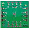
Evaluation boards
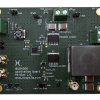
NEVB-NGD4300GC - 120 V, 4 A half-bridge gate driver evaluation board
NEVB-NMUX1309 - Bi-directional 4:1 analog multiplexer evaluation board
.png)
NEVB-NEX80806DA - 85-264 Vac to 24 Vdc, 1 A flyback converter evaluation board
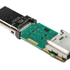
NEVB21-USBC1 - USB Type-C ESD protection evaluation board
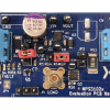
NEVB-NPS3102B - 12 V, 2-13.5 A, 17 mΩ auto-retry eFuse evaluation board
Reference designs
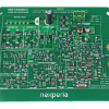
Nexperia H-bridge motor controller power supply circuit
.png)
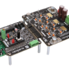
NEVB-MTR1-KIT1 – 1kW, 12-48 V BLDC motor driver kit