


- Block diagram
- Design considerations
- Design resources
- Product listing
- Support
Block diagram
Highlighted components are Nexperia focus products.
AC/DC conversion
Power management
Gate drive circuit
Inverter stage
Communications interface
Signal processing
Sensor interface
Aux power supply
Recommended products (8)
Select a component
To view more information about the Nexperia components used in this application, please select a component above or click on a component (highlighted in blue) in the block diagram.
Design considerations
- Switching losses versus conduction losses dominate device choice, so need to select MOSFETs based on RDS(on) and QG/Qoss trade-off.
- High-side gate driving and layout become critical for reliability. Bootstrap / driver must handle dV/dt, dead-time and Miller turn-on immunity. Poor layout or weak drivers lead to shoot-through and EMI.
- Regenerative operation drives DC bus and protection design so braking and bidirectional power flow require bus overvoltage handling (TVS, braking or control) and sufficient capacitor sizing.
- Fast edges require controlled gate resistance, snubbing and tight layout to avoid overshoot, false turn-on and compliance issues.
Design resources
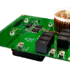
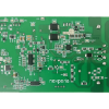
Evaluation boards
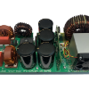
NX-HB-GAN039-650NBB-BSCUL - 400 V, 3.5 kW GaN FET (bottom-side cooled) half-bridge evaluation board
.png)
NX-HB-GAN03R2-100CBE-BSC 60V, 350 W GaN bottom-side cooled half-bridge evaluation board
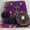
GAN039-650NTB - 4 kW, 85-265 Vac analog bridgeless totem-pole PFC evaluation board
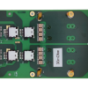
NEVB-NSF-XPAK-A - 1200 V SiC MOSFET (X.PAK) dual half-bridge evaluation board
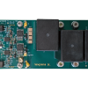
NEVB-HB-NSFD7-A - 1200 V SiC MOSFET (TO-263-7 ) double-pulse half-bridge evaluation board
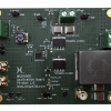
NEVB-NEX80806DA - 85-264 Vac to 24 Vdc, 1 A flyback converter evaluation board
Reference designs
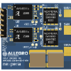
Allegro AHV85110 evaluation board
Broadcom GAN039-650NBB half bridge evaluation board
Nexperia 90-264 Vac, 24Vdc, 10A, 240W PFC and LLC reference design board