


74HC259-Q100; 74HCT259-Q100
8-bit addressable latch
The 74HC259-Q100; 74HCT259-Q100 is an 8-bit addressable latch. The device features four modes of operation. In the addressable latch mode, data on the D input is written into the latch addressed by the inputs A0 to A3. The addressed latch will follow the data input, non-addressed latches will retain their previous states. In memory mode, all latches retain their previous states and are unaffected by the data or address inputs. In the 3-to-8 decoding or demultiplexing mode, the addressed output follows the D input and all other outputs are LOW. In the reset mode, all outputs are forced LOW and unaffected by the data or address inputs. Inputs include clamp diodes. This enables the use of current limiting resistors to interface inputs to voltages in excess of VCC.
This product has been qualified to the Automotive Electronics Council (AEC) standard Q100 (Grade 1) and is suitable for use in automotive applications.
Features and benefits
Automotive product qualification in accordance with AEC-Q100 (Grade 1)
Specified from -40 °C to +85 °C and from -40 °C to +125 °C
Wide supply voltage range from 2.0 V to 6.0 V
Latch-up performance exceeds 100 mA per JESD 78 Class II Level B
Complies with JEDEC standards:
- JESD8C (2.7 V to 3.6 V)
- JESD7A (2.0 V to 6.0 V)
Combined demultiplexer and 8-bit latch
Serial-to-parallel capability
Output from each storage bit available
Random (addressable) data entry
Easily expandable
Common reset input
Useful as a 3-to-8 active HIGH decoder
Input levels:
For 74HC259-Q100: CMOS level
For 74HCT259-Q100: TTL level
ESD protection:
HBM: ANSI/ESDA/JEDEC JS-001 class 2 exceeds 2000 V
CDM: ANSI/ESDA/JEDEC JS-002 class C3 exceeds 1000 V
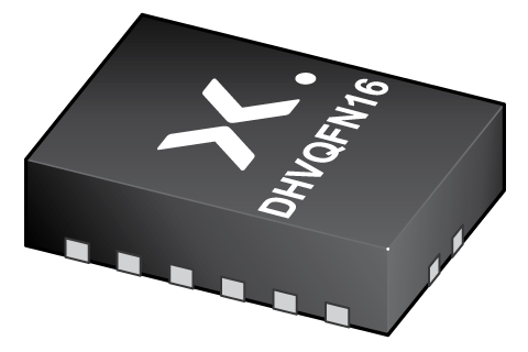
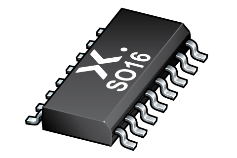
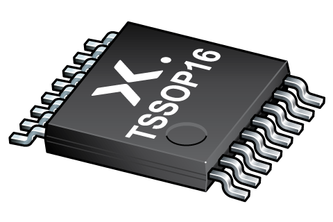
Multiple package options
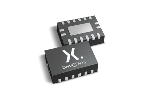
DHVQFN package with Side-Wettable Flanks enabling Automatic Optical Inspection (AOI) of solder joints
Parametrics
| Type number | VCC (V) | Logic switching levels | Output drive capability (mA) | tpd (ns) | Power dissipation considerations | Tamb (°C) | Ψth(j-top) (K/W) | Rth(j-c) (K/W) | Package name |
|---|---|---|---|---|---|---|---|---|---|
| 74HC259BQ-Q100 | 2.0 - 6.0 | CMOS | ± 5.2 | 18 | low | -40~125 | 10.8 | 57 | DHVQFN16 |
| 74HC259D-Q100 | 2.0 - 6.0 | CMOS | ± 5.2 | 18 | low | -40~125 | 7.7 | 47 | SO16 |
| 74HC259PW-Q100 | 2.0 - 6.0 | CMOS | ± 5.2 | 18 | low | -40~125 | 3.6 | 49.9 | TSSOP16 |
| 74HCT259BQ-Q100 | 4.5 - 5.5 | TTL | ± 4 | 20 | low | -40~125 | 10.8 | 57 | DHVQFN16 |
| 74HCT259D-Q100 | 4.5 - 5.5 | TTL | ± 4 | 20 | low | -40~125 | 7.7 | 47 | SO16 |
| 74HCT259PW-Q100 | 4.5 - 5.5 | TTL | ± 4 | 20 | low | -40~125 | 3.6 | 49.9 | TSSOP16 |
Package
| Type number | Orderable part number, (Ordering code (12NC)) | Status | Marking | Package | Package information | Reflow-/Wave soldering | Packing |
|---|---|---|---|---|---|---|---|
| 74HC259BQ-Q100 | 74HC259BQ‑Q100,115 (935298821115) |
Active | HC259 |
DHVQFN16 (SOT763-1) |
SOT763-1 | SOT763-1_115 | |
| 74HC259D-Q100 | 74HC259D‑Q100,118 (935298822118) |
Active | 74HC259D |
SO16 (SOT109-1) |
SOT109-1 |
SO-SOJ-REFLOW
SO-SOJ-WAVE WAVE_BG-BD-1 |
SOT109-1_118 |
| 74HC259PW-Q100 | 74HC259PW‑Q100,118 (935298823118) |
Active | HC259 |
TSSOP16 (SOT403-1) |
SOT403-1 |
SSOP-TSSOP-VSO-WAVE
|
SOT403-1_118 |
| 74HCT259BQ-Q100 | 74HCT259BQ‑Q100,11 (935298824115) |
Active | HCT259 |
DHVQFN16 (SOT763-1) |
SOT763-1 | SOT763-1_115 | |
| 74HCT259D-Q100 | 74HCT259D‑Q100,118 (935298825118) |
Active | 74HCT259D |
SO16 (SOT109-1) |
SOT109-1 |
SO-SOJ-REFLOW
SO-SOJ-WAVE WAVE_BG-BD-1 |
SOT109-1_118 |
| 74HCT259PW-Q100 | 74HCT259PW‑Q100,11 (935298826118) |
Active | HCT259 |
TSSOP16 (SOT403-1) |
SOT403-1 |
SSOP-TSSOP-VSO-WAVE
|
SOT403-1_118 |
Environmental information
| Type number | Orderable part number | Chemical content | RoHS | RHF-indicator |
|---|---|---|---|---|
| 74HC259BQ-Q100 | 74HC259BQ‑Q100,115 | 74HC259BQ-Q100 |
|
|
| 74HC259D-Q100 | 74HC259D‑Q100,118 | 74HC259D-Q100 |
|
|
| 74HC259PW-Q100 | 74HC259PW‑Q100,118 | 74HC259PW-Q100 |
|
|
| 74HCT259BQ-Q100 | 74HCT259BQ‑Q100,11 | 74HCT259BQ-Q100 |
|
|
| 74HCT259D-Q100 | 74HCT259D‑Q100,118 | 74HCT259D-Q100 |
|
|
| 74HCT259PW-Q100 | 74HCT259PW‑Q100,11 | 74HCT259PW-Q100 |
|
|
Documentation (20)
| File name | Title | Type | Date |
|---|---|---|---|
| 74HC_HCT259_Q100 | 8-bit addressable latch | Data sheet | 2024-03-11 |
| AN11044 | Pin FMEA 74HC/74HCT family | Application note | 2019-01-09 |
| AN90063 | Questions about package outline drawings | Application note | 2025-10-22 |
| SOT763-1 | 3D model for products with SOT763-1 package | Design support | 2019-10-03 |
| SOT109-1 | 3D model for products with SOT109-1 package | Design support | 2020-01-22 |
| SOT403-1 | 3D model for products with SOT403-1 package | Design support | 2020-01-22 |
| hc259 | 74HC259 IBIS model | IBIS model | 2022-10-21 |
| hct259 | 74HCT259 IBIS model | IBIS model | 2022-10-21 |
| Nexperia_package_poster | Nexperia package poster | Leaflet | 2020-05-15 |
| DHVQFN16_SOT763-1_mk | plastic, dual in-line compatible thermal enhanced very thin quad flat package; 16 terminals; 0.5 mm pitch; 3.5 mm x 2.5 mm x 0.85 mm body | Marcom graphics | 2017-01-28 |
| SO16_SOT109-1_mk | plastic, small outline package; 16 leads; 1.27 mm pitch; 9.9 mm x 3.9 mm x 1.35 mm body | Marcom graphics | 2017-01-28 |
| TSSOP16_SOT403-1_mk | plastic, thin shrink small outline package; 16 leads; 0.65 mm pitch; 5 mm x 4.4 mm x 1.1 mm body | Marcom graphics | 2017-01-28 |
| SOT763-1 | plastic, leadless dual in-line compatible thermal enhanced very thin quad flat package; 16 terminals; 0.5 mm pitch; 3.5 mm x 2.5 mm x 1 mm body | Package information | 2023-05-11 |
| SOT109-1 | plastic, small outline package; 16 leads; 1.27 mm pitch; 9.9 mm x 3.9 mm x 1.75 mm body | Package information | 2023-11-07 |
| SOT403-1 | plastic, thin shrink small outline package; 16 leads; 5 mm x 4.4 mm x 1.2 mm body | Package information | 2023-11-08 |
| SO-SOJ-REFLOW | Footprint for reflow soldering | Reflow soldering | 2009-10-08 |
| HCT_USER_GUIDE | HC/T User Guide | User manual | 1997-10-31 |
| SO-SOJ-WAVE | Footprint for wave soldering | Wave soldering | 2009-10-08 |
| WAVE_BG-BD-1 | Wave soldering profile | Wave soldering | 2021-09-08 |
| SSOP-TSSOP-VSO-WAVE | Footprint for wave soldering | Wave soldering | 2009-10-08 |
Support
If you are in need of design/technical support, let us know and fill in the answer form we'll get back to you shortly.
Models
| File name | Title | Type | Date |
|---|---|---|---|
| SOT763-1 | 3D model for products with SOT763-1 package | Design support | 2019-10-03 |
| SOT109-1 | 3D model for products with SOT109-1 package | Design support | 2020-01-22 |
| SOT403-1 | 3D model for products with SOT403-1 package | Design support | 2020-01-22 |
| hc259 | 74HC259 IBIS model | IBIS model | 2022-10-21 |
| hct259 | 74HCT259 IBIS model | IBIS model | 2022-10-21 |
Ordering, pricing & availability
Sample
As a Nexperia customer you can order samples via our sales organization.
If you do not have a direct account with Nexperia our network of global and regional distributors is available and equipped to support you with Nexperia samples. Check out the list of official distributors.