
Features and benefits
-
Optimized for low voltage applications over a wide supply voltage range from 1.0 V to 3.6 V
-
Accepts TTL input levels between VCC = 2.7 V and VCC = 3.6 V
-
Typical output ground bounce < 0.8 V at VCC = 3.3 V and Tamb = 25 °C
-
Typical HIGH-level output voltage (VOH) undershoot: > 2 V at VCC = 3.3 V and Tamb = 25 °C
-
CMOS low power dissipation
-
Direct interface with TTL levels
-
Latch-up performance exceeds 100 mA per JESD 78 Class II Level B
-
Complies with JEDEC standards
-
JESD8-7 (1.65 V to 1.95 V)
-
JESD8-5 (2.3 V to 2.7 V)
-
JESD8C (2.7 V to 3.6 V)
-
-
ESD protection:
-
HBM JESD22-A114E exceeds 2000 V
-
MM JESD22-A115-A exceeds 200 V
-
-
Specified from -40 °C to +85 °C and from -40 °C to +125 °C
Applications
-
Serial-to-parallel data conversion
-
Remote control holding register
Parametrics
| Type number | Product status | VCC (V) | Logic switching levels | Output drive capability (mA) | tpd (ns) | fmax (MHz) | Nr of bits | Power dissipation considerations | Tamb (°C) | Rth(j-a) (K/W) | Ψth(j-top) (K/W) | Rth(j-c) (K/W) | Package name |
|---|---|---|---|---|---|---|---|---|---|---|---|---|---|
| 74LV4094D | Production | 1.0 - 3.6 | TTL | ± 6 | 14 | 95 | 8 | low | -40~125 | 81 | 4.9 | 40.3 | SO16 |
| 74LV4094PW | Production | 1.0 - 3.6 | TTL | ± 6 | 14 | 95 | 8 | low | -40~125 | 115 | 2.4 | 44 | TSSOP16 |
Package
| Type number | Package | Package information | Reflow-/Wave soldering | Packing | Status | Marking | Orderable part number, (Ordering code (12NC)) |
|---|---|---|---|---|---|---|---|
| 74LV4094D | 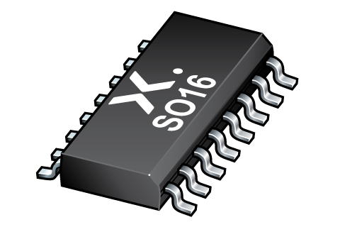 SO16 (SOT109-1) | SOT109-1 | SO-SOJ-REFLOW SO-SOJ-WAVE | SOT109-1_118 | Active | 74LV4094D | 74LV4094D,118 ( 9350 880 40118 ) |
| 74LV4094PW | 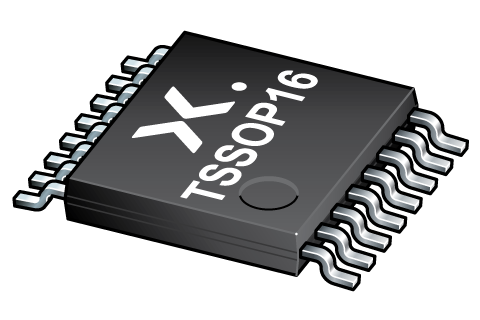 TSSOP16 (SOT403-1) | SOT403-1 | SSOP-TSSOP-VSO-WAVE | SOT403-1_118 | Active | LV4094 | 74LV4094PW,118 ( 9351 750 20118 ) |
The variants in the table below are discontinued. See the table Discontinuation information for more information.
| Type number | Package | Package information | Reflow-/Wave soldering | Packing | Status | Marking | Orderable part number, (Ordering code (12NC)) |
|---|---|---|---|---|---|---|---|
| 74LV4094PW | TSSOP16 (SOT403-1) | SOT403-1 | SSOP-TSSOP-VSO-WAVE | SOT403-1_112 | Withdrawn / End-of-life | LV4094 | 74LV4094PW,112 ( 9351 750 20112 ) |
Discontinuation information
| Type number | Orderable part number, (Ordering code (12NC)) | Last time buy date | Last time delivery date | Replacement product | Status | Comments |
|---|---|---|---|---|---|---|
| 74LV4094D | 935088040112 | 2021-12-31 | 2022-06-30 | 74LV4094D | ||
| 74LV4094PW | 935175020112 | 2021-12-31 | 2022-06-30 | 74LV4094PW |
Environmental information
| Type number | Orderable part number | Chemical content | RoHS | RHF-indicator | Leadfree conversion date |
|---|---|---|---|---|---|
| 74LV4094D | 74LV4094D,118 | 74LV4094D | week 6, 2004 | ||
| 74LV4094PW | 74LV4094PW,118 | 74LV4094PW | week 17, 2005 |
The variants in the table below are discontinued. See the table Discontinuation information for more information.
| Type number | Orderable part number | Chemical content | RoHS | RHF-indicator | Leadfree conversion date |
|---|---|---|---|---|---|
| 74LV4094PW | 74LV4094PW,112 | 74LV4094PW | week 17, 2005 |
Documentation (8)
| File name | Title | Type | Date |
|---|---|---|---|
| 74LV4094 | 8-stage shift-and-store bus register | Data sheet | 2021-03-18 |
| Nexperia_Selection_guide_2023 | Nexperia Selection Guide 2023 | Selection guide | 2023-05-10 |
| SO-SOJ-WAVE | Footprint for wave soldering | Wave soldering | 2009-10-08 |
| SO-SOJ-REFLOW | Footprint for reflow soldering | Reflow soldering | 2009-10-08 |
| WAVE_BG-BD-1 | Wave soldering profile | Wave soldering | 2021-09-08 |
| SOT109-1 | plastic, small outline package; 16 leads; 1.27 mm pitch; 9.9 mm x 3.9 mm x 1.75 mm body | Package information | 2023-11-07 |
| SOT403-1 | plastic, thin shrink small outline package; 16 leads; 5 mm x 4.4 mm x 1.2 mm body | Package information | 2023-11-08 |
| SSOP-TSSOP-VSO-WAVE | Footprint for wave soldering | Wave soldering | 2009-10-08 |
Support
If you are in need of design/technical support, let us know and fill in the answer form, we'll get back to you shortly.
Ordering, pricing & availability
Sample
As a Nexperia customer you can order samples via our sales organization or directly via our Online Sample Store: https://extranet.nexperia.com.
Sample orders normally take 2-4 days for delivery.
If you do not have a direct account with Nexperia our network of global and regional distributors is available and equipped to support you with Nexperia samples.