


74LVC2G00
Dual 2-input NAND gate
The 74LVC2G00 is a dual 2-input NAND gate. Inputs can be driven from either 3.3 V or 5 V devices. This feature allows the use of these devices as translators in mixed 3.3 V and 5 V environments.
Schmitt-trigger action at all inputs makes the circuit tolerant of slower input rise and fall times.
This device is fully specified for partial power down applications using IOFF. The IOFF circuitry disables the output, preventing the potentially damaging backflow current through the device when it is powered down.
Features and benefits
Wide supply voltage range from 1.65 V to 5.5 V
5 V tolerant outputs for interfacing with 5 V logic
High noise immunity
±24 mA output drive (VCC = 3.0 V)
CMOS low power dissipation
IOFF circuitry provides partial Power-down mode operation
Complies with JEDEC standard:
JESD8-7 (1.65 V to 1.95 V)
JESD8-5 (2.3 V to 2.7 V)
JESD8-B/JESD36 (2.7 V to 3.6 V)
Latch-up performance exceeds 250 mA
Direct interface with TTL levels
Overvoltage tolerant inputs to 5.5 V
ESD protection:
HBM: ANSI/ESDA/JEDEC JS-001 class 2 exceeds 2000 V
CDM: ANSI/ESDA/JEDEC JS-002 class C3 exceeds 1000 V
Multiple package options
Specified from -40 °C to +85 °C and -40 °C to +125 °C
Parametrics
| Type number | VCC (V) | Logic switching levels | Output drive capability (mA) | tpd (ns) | fmax (MHz) | Nr of bits | Power dissipation considerations | Tamb (°C) | Rth(j-a) (K/W) | Ψth(j-top) (K/W) | Rth(j-c) (K/W) | Package name |
|---|---|---|---|---|---|---|---|---|---|---|---|---|
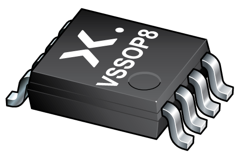
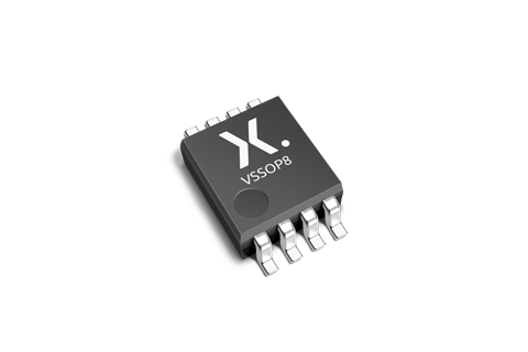
| 74LVC2G00DC | 1.65 - 5.5 | CMOS/LVTTL | ± 32 | 2.2 | 175 | 2 | low | -40~125 | 200 | 32.4 | 110 | VSSOP8 |
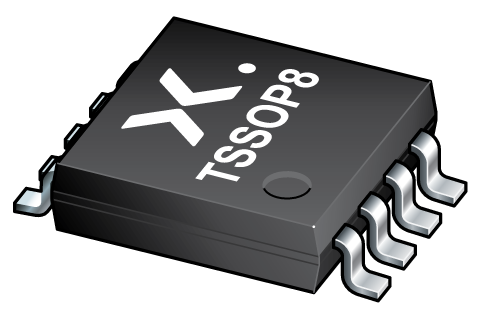
| 74LVC2G00DP | 1.65 - 5.5 | CMOS/LVTTL | ± 32 | 2.2 | 175 | 2 | low | -40~125 | 210 | 18.8 | 104 | TSSOP8 |
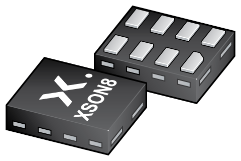
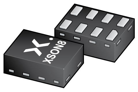
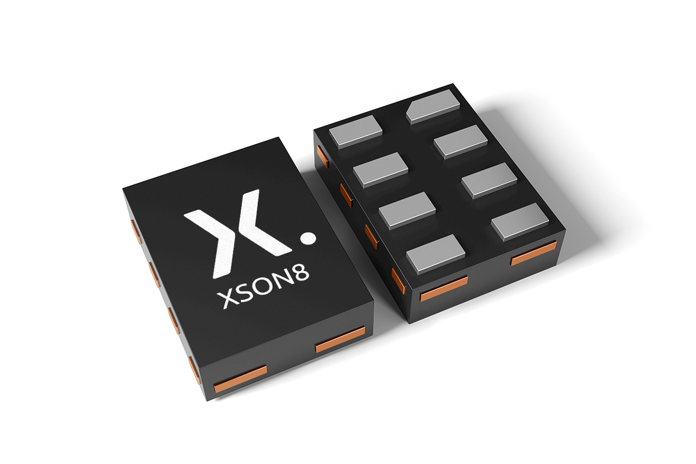
| 74LVC2G00GN | 1.65 - 5.5 | CMOS/LVTTL | ± 32 | 2.2 | 175 | 2 | low | -40~125 | 231 | 9.5 | 142 | XSON8 |
| 74LVC2G00GS | 1.65 - 5.5 | CMOS/LVTTL | ± 32 | 2.2 | 175 | 2 | low | -40~125 | 269 | 9.7 | 141 | XSON8 |
| 74LVC2G00GT | 1.65 - 5.5 | CMOS/LVTTL | ± 32 | 2.2 | 175 | 2 | low | -40~125 | 317 | 5.6 | 150 | XSON8 |
| 74LVC2G00GX | 1.65 - 5.5 | CMOS/LVTTL | ± 32 | 2.2 | 175 | 2 | low | -40~125 | X2SON8 |
Package
| Type number | Orderable part number, (Ordering code (12NC)) | Status | Marking | Package | Package information | Reflow-/Wave soldering | Packing |
|---|---|---|---|---|---|---|---|
| 74LVC2G00DC | 74LVC2G00DC,125 (935275224125) |
Active | V00 |
VSSOP8 (SOT765-1) |
SOT765-1 | SOT765-1_125 | |
| 74LVC2G00DP | 74LVC2G00DP,125 (935273581125) |
Active | V2G00 |
TSSOP8 (SOT505-2) |
SOT505-2 | SOT505-2_125 | |
| 74LVC2G00GN | 74LVC2G00GN,115 (935292236115) |
Active | VA |
XSON8 (SOT1116) |
SOT1116 | SOT1116_115 | |
| 74LVC2G00GS | 74LVC2G00GS,115 (935292381115) |
Active | VA |
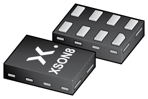
XSON8 (SOT1203) |
SOT1203 | SOT1203_115 | |
| 74LVC2G00GT | 74LVC2G00GT,115 (935278918115) |
Active | V00 |
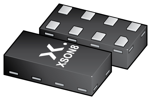
XSON8 (SOT833-1) |
SOT833-1 | SOT833-1_115 | |
| 74LVC2G00GX | 74LVC2G00GXX (935308444115) |
Active | VA |
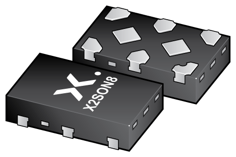
X2SON8 (SOT1233-2) |
SOT1233-2 | SOT1233-2_115 |
All type numbers in the table below are discontinued.
| Type number | Orderable part number, (Ordering code (12NC)) | Status | Marking | Package | Package information | Reflow-/Wave soldering | Packing |
|---|---|---|---|---|---|---|---|
| 74LVC2G00GD | 74LVC2G00GD,125 (935286852125) |
Obsolete | V00 Standard Procedure Standard Procedure |
XSON8 (SOT996-2) |
SOT996-2 | SOT996-2_125 | |
| 74LVC2G00GF | 74LVC2G00GF,115 (935291501115) |
Withdrawn / End-of-life |
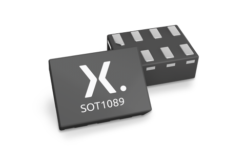
XSON8 (SOT1089) |
SOT1089 | SOT1089_115 | ||
| 74LVC2G00GM | 74LVC2G00GM,125 (935277235125) |
Obsolete | no package information | ||||
| 74LVC2G00GM,115 (935277235115) |
Obsolete | ||||||
Environmental information
| Type number | Orderable part number | Chemical content | RoHS | RHF-indicator |
|---|---|---|---|---|
| 74LVC2G00DC | 74LVC2G00DC,125 | 74LVC2G00DC |
|
|
| 74LVC2G00DP | 74LVC2G00DP,125 | 74LVC2G00DP |
|
|
| 74LVC2G00GN | 74LVC2G00GN,115 | 74LVC2G00GN |
|
|
| 74LVC2G00GS | 74LVC2G00GS,115 | 74LVC2G00GS |
|
|
| 74LVC2G00GT | 74LVC2G00GT,115 | 74LVC2G00GT |
|
|
| 74LVC2G00GX | 74LVC2G00GXX | 74LVC2G00GX |
|
|
All type numbers in the table below are discontinued.
| Type number | Orderable part number | Chemical content | RoHS | RHF-indicator |
|---|---|---|---|---|
| 74LVC2G00GD | 74LVC2G00GD,125 | 74LVC2G00GD |
|
|
| 74LVC2G00GF | 74LVC2G00GF,115 | 74LVC2G00GF |
|
|
| 74LVC2G00GM | 74LVC2G00GM,125 | 74LVC2G00GM |
|
|
| 74LVC2G00GM | 74LVC2G00GM,115 | 74LVC2G00GM |
|
|
Documentation (34)
| File name | Title | Type | Date |
|---|---|---|---|
| 74LVC2G00 | Dual 2-input NAND gate | Data sheet | 2024-05-08 |
| AN10161 | PicoGate Logic footprints | Application note | 2002-10-29 |
| AN11009 | Pin FMEA for LVC family | Application note | 2019-01-09 |
| AN90063 | Questions about package outline drawings | Application note | 2025-10-22 |
| 001aah748 | Block diagram: 74AUP2G00DC, 74AUP2G00GD, 74AUP2G00GM, 74AUP2G00GT, 74LVC2G00DC, 74LVC2G00DP, 74LVC2G00GD, 74LVC2G00GM, 74LVC2G00GT | Block diagram | 2009-11-03 |
| mna712 | Block diagram: 74LVC2G00DC, 74LVC2G00DP, 74LVC2G00GD, 74LVC2G00GM, 74LVC2G00GT | Block diagram | 2009-11-04 |
| Nexperia_document_guide_MiniLogic_PicoGate_201901 | PicoGate leaded logic portfolio guide | Brochure | 2019-01-07 |
| Nexperia_document_guide_MiniLogic_MicroPak_201808 | MicroPak leadless logic portfolio guide | Brochure | 2018-09-03 |
| SOT765-1 | 3D model for products with SOT765-1 package | Design support | 2020-01-22 |
| SOT505-2 | 3D model for products with SOT505-2 package | Design support | 2019-01-18 |
| SOT1089 | 3D model for products with SOT1089 package | Design support | 2019-10-07 |
| SOT1116 | 3D model for products with SOT1116 package | Design support | 2023-02-02 |
| SOT1203 | 3D model for products with SOT1203 package | Design support | 2023-02-02 |
| SOT833-1 | 3D model for products with SOT833-1 package | Design support | 2021-01-28 |
| SOT1233-2 | 3D model for products with SOT1233-2 package | Design support | 2021-01-28 |
| lvc2g00 | 74LVC2G00 IBIS model | IBIS model | 2014-10-20 |
| Nexperia_document_leaflet_Logic_X2SON_packages_062018 | X2SON ultra-small 4, 5, 6 & 8-pin leadless packages | Leaflet | 2018-06-05 |
| Nexperia_package_poster | Nexperia package poster | Leaflet | 2020-05-15 |
| VSSOP8_SOT765-1_mk | plastic, very thin shrink small outline package; 8 leads; 0.5 mm pitch; 2 mm x 2.3 mm x 1 mm body | Marcom graphics | 2017-01-28 |
| XSON8_SOT1089_mk | plastic, extremely thin small outline package; no leads; 8 terminals; 0.55 mm pitch; 1.35 mm x 1 mm x 0.5 mm body | Marcom graphics | 2017-01-28 |
| XSON8_SOT1203_mk | plastic, leadless extremely thin small outline package; 8 terminals; 0.35 mm pitch; 1.35 mm x 1 mm x 0.35 mm body | Marcom graphics | 2019-02-04 |
| REFLOW_BG-BD-1 | Reflow soldering profile | Other type | 2026-02-10 |
| SOT765-1 | plastic, very thin shrink small outline package; 8 leads; 0.5 mm pitch; 2 mm x 2.3 mm x 1 mm body | Package information | 2022-06-03 |
| SOT505-2 | plastic, thin shrink small outline package; 8 leads; 0.65 mm pitch; 3 mm x 3 mm x 1.1 mm body | Package information | 2022-06-03 |
| SOT996-2 | plastic, leadless extremely thin small outline package; 8 terminals; 0.5 mm pitch; 3 mm x 2 mm x 0.5 mm body | Package information | 2020-04-21 |
| SOT1089 | plastic, leadless extremely thin small outline package; 8 terminals; 0.35 mm pitch; 1.35 mm x 1 mm x 0.5 mm body | Package information | 2022-06-03 |
| SOT1116 | plastic, leadless extremely thin small outline package; 8 terminals; 0.3 mm pitch; 1.2 mm x 1 mm x 0.35 mm body | Package information | 2022-06-02 |
| SOT1203 | plastic, leadless extremely thin small outline package; 8 terminals; 0.35 mm pitch; 1.35 mm x 1 mm x 0.35 mm body | Package information | 2022-06-03 |
| SOT833-1 | plastic, leadless extremely thin small outline package; 8 terminals; 0.5 mm pitch; 1 mm x 1.95 mm x 0.5 mm body | Package information | 2022-06-03 |
| SOT1233-2 | plastic thermal enhanced extremely thin small outline package; no leads;8 terminals; body 1.35 x 0.8 x 0.32 mm | Package information | 2022-04-21 |
| MAR_SOT1089 | MAR_SOT1089 Topmark | Top marking | 2013-06-03 |
| MAR_SOT1116 | MAR_SOT1116 Topmark | Top marking | 2013-06-03 |
| MAR_SOT1203 | MAR_SOT1203 Topmark | Top marking | 2013-06-03 |
| MAR_SOT833 | MAR_SOT833 Topmark | Top marking | 2013-06-03 |
Support
If you are in need of design/technical support, let us know and fill in the answer form we'll get back to you shortly.
Models
| File name | Title | Type | Date |
|---|---|---|---|
| SOT765-1 | 3D model for products with SOT765-1 package | Design support | 2020-01-22 |
| SOT505-2 | 3D model for products with SOT505-2 package | Design support | 2019-01-18 |
| SOT1089 | 3D model for products with SOT1089 package | Design support | 2019-10-07 |
| SOT1116 | 3D model for products with SOT1116 package | Design support | 2023-02-02 |
| SOT1203 | 3D model for products with SOT1203 package | Design support | 2023-02-02 |
| SOT833-1 | 3D model for products with SOT833-1 package | Design support | 2021-01-28 |
| SOT1233-2 | 3D model for products with SOT1233-2 package | Design support | 2021-01-28 |
| lvc2g00 | 74LVC2G00 IBIS model | IBIS model | 2014-10-20 |
Ordering, pricing & availability
Sample
As a Nexperia customer you can order samples via our sales organization.
If you do not have a direct account with Nexperia our network of global and regional distributors is available and equipped to support you with Nexperia samples. Check out the list of official distributors.