
Features and benefits
-
Automotive product qualification in accordance with AEC-Q100 (Grade 1)
-
Specified from -40 °C to +85 °C and from -40 °C to +125 °C
-
-
Overvoltage tolerant inputs to 5.5 V
-
Wide supply voltage range from 1.2 V to 3.6 V
-
CMOS low power dissipation
-
MULTIBYTE flow-through standard pin-out architecture
-
Low inductance multiple power and ground pins for minimum noise and ground bounce
-
Direct interface with TTL levels
-
All data inputs have bus hold (74LVCH16245A-Q100 only)
-
IOFF circuitry provides partial Power-down mode operation
-
Complies with JEDEC standard:
-
JESD8-7A (1.65 V to 1.95 V)
-
JESD8-5A (2.3 V to 2.7 V)
-
JESD8-C/JESD36 (2.7 V to 3.6 V)
-
-
ESD protection:
-
HBM: ANSI/ESDA/JEDEC JS-001 class 2 exceeds 2000 V
-
CDM: ANSI/ESDA/JEDEC JS-002 class C3 exceeds 1000 V
-
Parametrics
| Type number | Product status | VCC (V) | Logic switching levels | Output drive capability (mA) | fmax (MHz) | Nr of bits | Power dissipation considerations | Tamb (°C) | Rth(j-a) (K/W) | Ψth(j-top) (K/W) | Rth(j-c) (K/W) | Package name |
|---|---|---|---|---|---|---|---|---|---|---|---|---|
| 74LVC16245ADGG-Q100 | Production | 1.2 - 3.6 | CMOS/LVTTL | +/- 24 | 175 | 16 | low | -40~125 | 82 | 1.9 | 36 | TSSOP48 |
| 74LVC16245ADGV-Q100 | Production | 1.2 - 3.6 | CMOS/LVTTL | +/- 24 | 175 | 16 | low | -40~125 | 82 | 0.0 | 36 | TVSOP48 |
| 74LVCH16245ADGG-Q100 | Production | 1.2 - 3.6 | CMOS/LVTTL | +/- 24 | 175 | 16 | low | -40~125 | 82 | 1.9 | 36 | TSSOP48 |
| 74LVCH16245ADGV-Q100 | Production | 1.2 - 3.6 | CMOS/LVTTL | +/- 24 | 175 | 16 | low | -40~125 | 82 | 0.0 | 36 | TVSOP48 |
Package
| Type number | Package | Package information | Reflow-/Wave soldering | Packing | Status | Marking | Orderable part number, (Ordering code (12NC)) |
|---|---|---|---|---|---|---|---|
| 74LVC16245ADGG-Q100 | 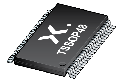 TSSOP48 (SOT362-1) | SOT362-1 | SSOP-TSSOP-VSO-WAVE | SOT362-1_118 | Active | LVC16245A | 74LVC16245ADGG-Q1J ( 9352 994 75118 ) |
| 74LVC16245ADGV-Q100 | 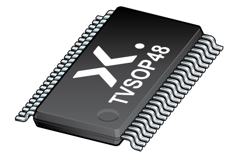 TVSOP48 (SOT480-1) | SOT480-1 | SOT480-1_118 | Active | 74LVC16245A | 74LVC16245ADGV-Q1J ( 9356 907 92118 ) | |
| 74LVCH16245ADGG-Q100 | TSSOP48 (SOT362-1) | SOT362-1 | SSOP-TSSOP-VSO-WAVE | SOT362-1_118 | Active | LVCH16245A | 74LVCH16245ADGG-QJ ( 9352 994 78118 ) |
| 74LVCH16245ADGV-Q100 | TVSOP48 (SOT480-1) | SOT480-1 | SOT480-1_118 | Active | 4LVCH16245A | 74LVCH16245ADGV-QJ ( 9356 907 97118 ) |
Environmental information
| Type number | Orderable part number | Chemical content | RoHS | RHF-indicator | Leadfree conversion date |
|---|---|---|---|---|---|
| 74LVC16245ADGG-Q100 | 74LVC16245ADGG-Q1J | 74LVC16245ADGG-Q100 | Always Pb-free | ||
| 74LVC16245ADGV-Q100 | 74LVC16245ADGV-Q1J | 74LVC16245ADGV-Q100 | week 25, 2019 | ||
| 74LVCH16245ADGG-Q100 | 74LVCH16245ADGG-QJ | 74LVCH16245ADGG-Q100 | Always Pb-free | ||
| 74LVCH16245ADGV-Q100 | 74LVCH16245ADGV-QJ | 74LVCH16245ADGV-Q100 | week 25, 2019 |
Documentation (10)
| File name | Title | Type | Date |
|---|---|---|---|
| 74LVC_LVCH16245A_Q100 | 16-bit bus transceiver with direction pin; 5 V tolerant; 3-state | Data sheet | 2024-04-23 |
| AN263 | Power considerations when using CMOS and BiCMOS logic devices | Application note | 2023-02-07 |
| AN11009 | Pin FMEA for LVC family | Application note | 2019-01-09 |
| lvch16245a | lvch16245a IBIS model | IBIS model | 2013-04-07 |
| lvc16245a | lvc16245a IBIS model | IBIS model | 2013-04-07 |
| Nexperia_document_leaflet_Logic_TVSOP48_16bitPortfolio_201903 | Smaller-footprint 16-bit logic with advanced features | Leaflet | 2019-03-29 |
| Nexperia_Selection_guide_2023 | Nexperia Selection Guide 2023 | Selection guide | 2023-05-10 |
| SOT480-1 | plastic, thin shrink small outline package; 48 leads; 0.4 mm pitch; 9.7 mm x 4.4 mm x 1.1 mm body | Package information | 2022-06-22 |
| SSOP-TSSOP-VSO-WAVE | Footprint for wave soldering | Wave soldering | 2009-10-08 |
| SOT362-1 | plastic thin shrink small outline package; 48 leads; body width 6.1 mm | Package information | 2024-01-05 |
Support
If you are in need of design/technical support, let us know and fill in the answer form, we'll get back to you shortly.
Models
| File name | Title | Type | Date |
|---|---|---|---|
| lvch16245a | lvch16245a IBIS model | IBIS model | 2013-04-07 |
| lvc16245a | lvc16245a IBIS model | IBIS model | 2013-04-07 |
Ordering, pricing & availability
Sample
As a Nexperia customer you can order samples via our sales organization or directly via our Online Sample Store: https://extranet.nexperia.com.
Sample orders normally take 2-4 days for delivery.
If you do not have a direct account with Nexperia our network of global and regional distributors is available and equipped to support you with Nexperia samples.