
Features and benefits
-
Automotive product qualification in accordance with AEC-Q100 (Grade 1)
-
Specified from -40 °C to +85 °C and from -40 °C to +125 °C
-
-
Wide supply voltage range from 1.65 V to 5.5 V
-
5 V tolerant inputs for interfacing with 5 V logic
-
High noise immunity
-
±24 mA output drive (VCC = 3.0 V)
-
CMOS low power consumption
-
Latch-up performance exceeds 250 mA
-
Direct interface with TTL levels
-
Inputs accept voltages up to 5 V
-
Complies with JEDEC standard:
-
JESD8-7 (1.65 V to 1.95 V)
-
JESD8-5 (2.3 V to 2.7 V)
-
JESD8-B/JESD36 (2.7 V to 3.6 V).
-
-
ESD protection:
-
HBM: ANSI/ESDA/JEDEC JS-001 class 2 exceeds 2000 V
-
CDM: ANSI/ESDA/JEDEC JS-002 class C3 exceeds 1000 V
-
Parametrics
| Type number | Product status | VCC (V) | Logic switching levels | Output drive capability (mA) | fmax (MHz) | Nr of bits | Power dissipation considerations | Tamb (°C) | Rth(j-a) (K/W) | Ψth(j-top) (K/W) | Rth(j-c) (K/W) | Package name |
|---|---|---|---|---|---|---|---|---|---|---|---|---|
| 74LVC1G16GW-Q100 | Production | 1.65 - 5.5 | CMOS/LVTTL | ± 32 | 175 | 1 | low | -40~125 | 319 | 88.0 | 188 | TSSOP5 |
Package
| Type number | Package | Package information | Reflow-/Wave soldering | Packing | Status | Marking | Orderable part number, (Ordering code (12NC)) |
|---|---|---|---|---|---|---|---|
| 74LVC1G16GW-Q100 | 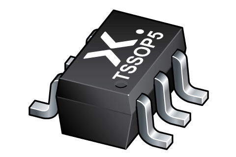 TSSOP5 (SOT353-1) | SOT353-1 | WAVE_BG-BD-1 | SOT353-1_125 | Active | Yr | 74LVC1G16GW-Q100H ( 9356 912 03125 ) |
Environmental information
| Type number | Orderable part number | Chemical content | RoHS | RHF-indicator | Leadfree conversion date |
|---|---|---|---|---|---|
| 74LVC1G16GW-Q100 | 74LVC1G16GW-Q100H | 74LVC1G16GW-Q100 |
Documentation (4)
| File name | Title | Type | Date |
|---|---|---|---|
| 74LVC1G16_Q100 | Single buffer | Data sheet | 2023-08-15 |
| lvc1g16 | 74LVC1G16 IBIS model | IBIS model | 2015-10-29 |
| WAVE_BG-BD-1 | Wave soldering profile | Wave soldering | 2021-09-08 |
| SOT353-1 | plastic thin shrink small outline package; 5 leads; body width 1.25 mm | Package information | 2022-11-15 |
Support
If you are in need of design/technical support, let us know and fill in the answer form, we'll get back to you shortly.
Models
| File name | Title | Type | Date |
|---|---|---|---|
| lvc1g16 | 74LVC1G16 IBIS model | IBIS model | 2015-10-29 |
Ordering, pricing & availability
Sample
As a Nexperia customer you can order samples via our sales organization or directly via our Online Sample Store: https://extranet.nexperia.com.
Sample orders normally take 2-4 days for delivery.
If you do not have a direct account with Nexperia our network of global and regional distributors is available and equipped to support you with Nexperia samples.