
- Product details
- Documentation
- Support
- Ordering
- Interactive data sheet
Product details
Features and benefits
-
Automotive product qualification in accordance with AEC-Q100 (Grade 1)
-
Specified from -40 °C to +85 °C and from -40 °C to +125 °C
-
-
Wide supply voltage range from 2.0 V to 6.0 V
- Schmitt-trigger inputs
- Low power consumption
- Typical supply current (ICC) of 100 nA
- Typical input leakage current (II) of ±10 nA
- ±7.8 mA output drive at 6 V
-
Combined demultiplexer and 8-bit latch
-
Serial-to-parallel capability
-
Output from each storage bit available
-
Random (addressable) data entry
-
Easily expandable
-
Common reset input
-
Useful as a 3-to-8 active HIGH decoder
- Latch-up performance exceeds 100 mA per JESD 78 Class II Level B
-
Complies with JEDEC standards:
- JESD7A (2.0 V to 6.0 V)
-
ESD protection:
-
HBM ANSI/ESDA/JEDEC JS-001 class 3A exceeds 4000 V
-
CDM ANSI/ESDA/JEDEC JS-002 class C3 exceeds 1500 V
-
-
Multiple package options
-
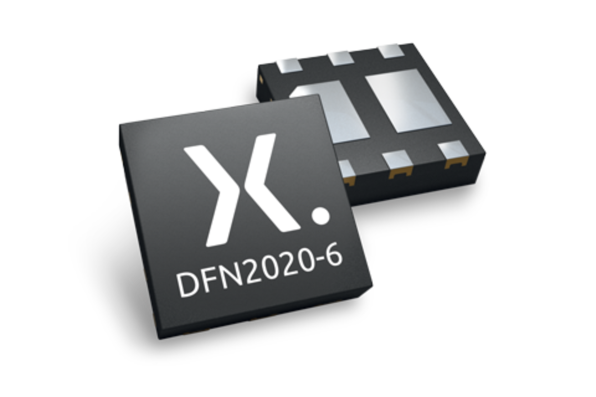
DHVQFN package with Side-Wettable Flanks enabling Automated Optical Inspection (AOI) of solder joints
Register once, drag and drop ECAD models into your CAD tool and speed up your design.
More informationQuality and reliability disclaimer
Support
Please contact us if you have any questions. If you are in need of design support, please fill in the technical support form, we will get back to you shortly.
Please visit our engineer exchange forum or contact us for further support.
Longevity
The Nexperia Longevity Program is aimed to provide our customers information from time to time about the expected time that our products can be ordered. The NLP is reviewed and updated regularly by our Executive Management Team. View our longevity program here.
Sample
As a Nexperia customer you can order samples via our sales organization.
If you do not have a direct account with Nexperia our network of global and regional distributors is available and equipped to support you with Nexperia samples. Check out the list of official distributors.
Interactive data sheet
How does it work?
The interactive data sheets are based on the Nexperia MOSFET precision electrothermal models. With our interactive data sheets you can simply specify your own conditions interactively. Start by changing the values of the conditions. You can do this by using the sliders in the condition fields. By dragging the sliders you will see how the MOSFET will perform at the new conditions set.
Interactive data sheet