


Power density, RDS(on) and miniaturization
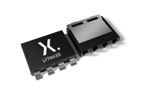
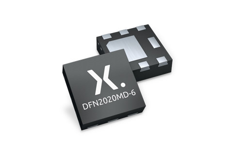
In virtually every application, getting the right balance of power density and RDS(on) in the right footprint is becoming increasingly critical. Nexperia offers a broad portfolio of N- and P-channel power MOSFETs, ranging from 12 V to 100 V and available in a wide range of space-saving and efficient package options. These range from the ultra-small DFN0603 MOSFET package for wearable applications through to our proven copper-clip LFPAK technology for the most challenging industrial designs. And as a long-term supplier to the automotive industry, you can be assured we maintain the highest quality and reliability standards.
Featured
%20(1).jpg)
Focus Packages
Latest news and blogs
.jpg)


.jpg)
.jpg)


Parametric search
 Please wait, loading data...
 Get MOSFETs suggested based on your application
With over 900 products in our portfolio – you don’t need to be an expert in MOSFETs to select the device with the best performance for your requirements. Specify your application below, put in your conditions and get three MOSFETs suggested. The suggestions are based on results from spice simulations with the top three best performing devices shown.
Application note (32) |
|||
|---|---|---|---|
| File name | Title | Type | Date |
| AN90003.pdf | LFPAK MOSFET thermal design guide | Application note | 2026-02-12 |
| AN10273.pdf | Power MOSFET single-shot and repetitive avalanche ruggedness rating | Application note | 2026-02-12 |
| AN90034.pdf | Nexperia Precision Electrothermal models in SPICE and VHDL-AMS for Power MOSFETs | Application note | 2025-11-19 |
| AN90009.pdf | Leakage of small-signal MOSFETs | Application note | 2025-10-21 |
| AN50020.pdf | MOSFETs in Power Switch applications | Application note | 2025-10-21 |
| AN50019.pdf | Thermal boundary condition study on MOSFET packages and PCB substrates | Application note | 2025-10-21 |
| AN50001.pdf | Reverse battery protection in automotive applications | Application note | 2025-10-21 |
| AN11304.pdf | MOSFET load switch PCB with thermal measurement | Application note | 2025-10-21 |
| AN11158.pdf | Understanding power MOSFET data sheet parameters | Application note | 2025-10-21 |
| AN11156.pdf | Using Power MOSFET Zth Curves | Application note | 2025-10-21 |
| AN90059.pdf | Power MOSFET gate driver fundamentals | Application note | 2025-09-10 |
| AN90011.pdf | Half-bridge MOSFET switching and its impact on EMC | Application note | 2025-09-10 |
| AN50002.pdf | Automotive LED side light SEPIC DC-to-DC converter design example | Application note | 2025-09-10 |
| AN11261.pdf | RC Thermal Models | Application note | 2025-09-10 |
| AN11160.pdf | Designing RC Snubbers | Application note | 2025-09-10 |
| AN90046.pdf | CCPAK1212i Design Guide | Application note | 2025-09-08 |
| AN90016.pdf | Maximum continuous currents in NEXPERIA LFPAK power MOSFETs | Application note | 2025-09-08 |
| AN90001.pdf | Designing in MOSFETs for safe and reliable gate-drive operation | Application note | 2025-09-08 |
| AN50014.pdf | Understanding the MOSFET peak drain current rating | Application note | 2025-09-08 |
| AN50006.pdf | Power MOSFETs in linear mode | Application note | 2025-09-08 |
| AN11243.pdf | Failure signature of Electrical Overstress on Power MOSFETs | Application note | 2025-09-08 |
| AN50003.pdf | Driving solenoids in automotive applications | Application note | 2025-04-09 |
| AN50005_translated_20230317.pdf | 大電力アプリケーションにおけるパワーMOSFETの並列接続 | Application note | 2023-04-03 |
| AN50009.pdf | Power MOSFET applications in automotive BLDC and PMSM drives | Application note | 2022-07-05 |
| AN90032.pdf | Low temperature soldering, application study | Application note | 2022-02-22 |
| AN11158_ZH.pdf | Understanding power MOSFET data sheet parameters | Application note | 2021-01-04 |
| AN90023.pdf | Thermal performance of DFN packages | Application note | 2020-11-23 |
| AN90017.pdf | Load switches for mobile and computing applications | Application note | 2020-09-02 |
| AN90019.pdf | LFPAK MOSFET thermal resistance - simulation, test and optimization of PCB layout | Application note | 2020-07-20 |
| AN10441.pdf | Level shifting techniques in I2C-bus design | Application note | 2020-02-11 |
| AN11599.pdf | Using power MOSFETs in parallel | Application note | 2016-07-13 |
| AN11119.pdf | Medium power small-signal MOSFETs in DC-to-DC conversion | Application note | 2013-05-07 |
Leaflet (18) |
|||
| File name | Title | Type | Date |
| nexperia_document_CCPAK_MOSFETs_2025.pdf | CCPAK MOSFETs leaflet | Leaflet | 2025-09-18 |
| nexperia_document_CCPAK_MOSFETs_2025-CHN.pdf | CCPAK MOSFETs leaflet CHN | Leaflet | 2025-09-18 |
| nexperia_document_leaflet_IDs_2024_CHN.pdf | nexperia_document_leaflet_IDs_2024_CHN | Leaflet | 2024-09-12 |
| nexperia_document_leaflet_IDs_2024.pdf | nexperia_document_leaflet_IDs_2024 | Leaflet | 2024-09-12 |
| nexperia_document_leaflet_DFN_Packages_Diodes_Transistors_ESD_Protection.pdf | DFN Packages Diodes Transistors ESD Protection | Leaflet | 2024-08-26 |
| nexperia_document_leaflet_DFN2020MD-6_2023.pdf | DFN2020MD-6 Leadless package with side-wettable flanks | Leaflet | 2023-09-19 |
| nexperia_document_leaflet_DFN2020MD-6_2023-CHN.pdf | 带有侧边可湿焊盘的无引脚封装 | Leaflet | 2023-09-19 |
| nexperia_document_leaflet_SsMOS_for_mobile_2022.pdf | High volume small-signal MOSFETs for mobile and portables, in WLCSP and leadless DFN packages | Leaflet | 2022-07-04 |
| nexperia_document_leaflet_SsMOS_for_mobile_2022-CHN.pdf | 适合移动和便携式设备的 大批量小信号MOSFET, 采用WLCSP和无引脚DFN封装 | Leaflet | 2022-07-04 |
| nexperia_document_leaflet_LFPAK88_2022_CHN.pdf | LFPAK88 将功率密度提升到新高度 | Leaflet | 2022-03-10 |
| nexperia_document_leaflet_LFPAK88_2022.pdf | LFPAK88 - Driving power-density to the next level | Leaflet | 2022-03-09 |
| nexperia_document_leaflet_DFN0606_LR_2020.pdf | DFN0606 | Leaflet | 2020-04-15 |
| nexperia_document_leaflet_DFN0606_CHN_2020.pdf | DFN0606 Chinese Translation | Leaflet | 2020-04-15 |
| Nexperia_Document_Leaflet_LFPAK33_12022020_CH.pdf | LFPAK33 leaflet | Leaflet | 2020-03-25 |
| Nexperia_Document_Leaflet_LFPAK33_12022020.pdf | LFPAK33 shrinking the power footprint | Leaflet | 2020-03-25 |
| nexperia_document_leaflet_WLCSP_201803_CHN.pdf | WLCSP Chinese Translation | Leaflet | 2018-04-25 |
| nexperia_document_leaflet_WLCSP_201803.pdf | Small-signal MOSFETs in WLCSP - Smallest size - lowest RDS(on) | Leaflet | 2018-04-25 |
| nexperia_document_leaflet_LFPAK56D_factsheet_LR_201708.pdf | LFPAK56D the ultimate dual MOSFET | Leaflet | 2017-08-17 |
Marcom graphics (1) |
|||
| File name | Title | Type | Date |
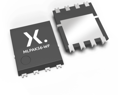
| LFPAK56_SOT669_mk.png | plastic, single-ended surface-mounted package; 4 terminals; 4.9 mm x 4.45 mm x 1 mm body | Marcom graphics | 2017-01-28 |
Selection guide (1) |
|||
| File name | Title | Type | Date |
| Nexperia_Selection_Guide_2025.pdf | Nexperia selection guide 2025 | Selection guide | 2025-05-16 |
Technical note (3) |
|||
| File name | Title | Type | Date |
| TN00008.pdf | Power MOSFET frequently asked questions and answers | Technical note | 2025-09-10 |
| TN90002.pdf | H-bridge motor controller design using Nexperia discrete semiconductors and logic ICs | Technical note | 2025-02-10 |
| TN90001.pdf | LFPAK MOSFET thermal resistance Rth(j-a) simulation, test and optimisation of PCB layout | Technical note | 2018-05-17 |
User manual (3) |
|||
| File name | Title | Type | Date |
| Nexperia_document_book_MOSFETGaNFETApplicationHandbook_2020.pdf | MOSFET & GaN FET Application Handbook | User manual | 2020-11-05 |
| The_Power_MOSFET_Handbook_Chinese_Version_201808.pdf | The Power MOSFET Handbook - Chinese Version 201808 | User manual | 2019-11-12 |
| UM90001.pdf | Store and transport requirements | User manual | 2018-04-06 |
White paper (1) |
|||
| File name | Title | Type | Date |
| Nexperia_document_whitepaper_DFN_Wave_Soldering_2020.pdf | Whitepaper: Can DFNs be successfully wave soldered? | White paper | 2020-09-01 |
Please contact us if you have any questions. If you are in need of design support, please fill in the technical support form, we will get back to you shortly.
Please visit our engineer exchange forum or contact us for further support.
Frequently Asked Questions
The VGS rating of 10 V given to Trench 6 logic level MOSFETs is driven by our <1 ppm failure rate targets and was rated to the best industry practices at the time. The ppm failure figures are not given in any data sheet nor are they part of AEC-Q101 qualification. In other words, two devices can both be qualified to AEC-Q101 and still have different ppm failure rate figures.
Methods of defining, characterising and protecting these ratings have improved and there is now a possibility to operate beyond the given rating of 10 V. This will be a function of time, voltage and temperature. For further explanation see below; more details are available in Nexperia application note AN90001.
The rating is based on meeting AEC-Q101 requirements, as it is with previous generations. However, Nexperia has developed a new testing methodology which ensures <1 ppm failure rates over lifetime at the rated VGS. This has been applied to Trench9 and its VGS rating is set to meet this new requirement. Detailed explanation can be found in AN90001
The method for setting the Zth curve has changed between the Trench generation 3 parts (2008) and Trench generation 6 (2012). The die size is also different which changes the Zth and Rth characteristics.
This understanding is correct. To ensure reliability of the MOSFET, always limit the maximum junction temperature to 175 °C.
The customer is trying to achieve a Rth(j-amb) = 60 K/W using a dual N channel LFPAK56 (SOT1205).
Rth(j-amb) = Rth(j-mb) + Rth(mb-amb)
Rth(j-mb) is in Nexperia’s control (it is a function of the die size and package design, for example the bigger the die the lower the Rth(j-mb)). Rth(mb-amb) is a function of the PCB design and the thermal management scheme and is not under the control of Nexperia. A very good multilayer FR4 design with thermal vias would be around 30 - 40 K/W.
The Rth(j-amb) is dependent on the PCB design. As MOSFET manufacturers we do not determine this part of the system and the value would be meaningless, therefore. We have provided some examples in our application notes, please see LFPAK thermal design guide AN90003.
Rth(j-mb) tells you the temperature difference between the junction and mounting base for a given power profile. Because of the power dissipation the mounting base to ambient path will also heat up, causing the junction temperature to rise further. The junction to ambient is the full thermal path that needs to be considered and is a function of the PCB design too, please see AN90003 for more details.
The drain tab (mounting base) and source leads are the two main paths through which a down side cooling package dissipates heat. In fact, contrarily to some through hole packages (like TO-220), SMD packages such as LFPAK and D2PAK get rid of all the heat through the PCB. Hot air rises from the board and envelopes the device lowering the efficiency and thus the efficacy of any heatsink attached to the top of the plastic case. Instead, when a substantial power needs to be dissipated, copper traces, vias and planes are employed in order to lower as much as possible the Rth(j-a) of a device.
FloTHERM simulations and measurements carried out using LFPAK56 and variable power dissipation and PCB copper area show how, in steady state conditions, temperature taken on the top center of the case is, within a reasonably low accuracy, very similar to the junction temperature. This result is not due to heat being dissipated from the top of the case but rather from the one coming out of the PCB that increases the temperature of the surrounding air immediately close to the device, up to almost that of the junction.
Conduction is the predominant phenomena regulating heat flow from junction to mounting base. The resulting resistance is inversely proportional to the cross sectional area of the medium through which it propagates (die area) and directly to its thickness (drain tab). Given an LFPAK56E and an LFPAK88 with the same die size the former has lower Rth(j-mb) because the thickness of its drain tab is lower. It is worth noting, however, that the thermal path doesn't end here and that the LFPAK88 shows better thermal performances due to its lower Rth(j-amb) given by a much larger drain tab.
For a given die size the LFPAK88 shows an overall better transient thermal impedance Zth(j-mb).
The data sheet states the IS capability for the diode. The power constraints are the same as for the MOSFET conduction. The diode is an integral part of the MOSFET structure. They are in effect the same size and have the same thermal properties. The MOSFET can carry the same current through the channel or in reverse through the body diode. The maximum steady state current in the diode is dependent on the total allowed power loss for the device. However, the diode current may be different from the channel current because the power dissipation may be different under the 2 modes of operation.
When a MOSFET transitions from diode conduction to blocking state there is an additional loss, called the diode recovery charge (Qr). The Qr needs to be factored in the switching loss calculation of the application for accurate analysis. This switching transition also impacts on the EMC performance and needs careful consideration - see AN90011 and TN90003 for more details.
The most important factor in current derating or power derating is junction temperature. Tj is a function of power dissipation. Power dissipation is a function of ID current and on-state resistance (P = I^2 × R) when operating in the fully enhanced mode. It is the product of ID and VDS when operating between on and off states. The RDS(on) of a MOSFET, increases with increase in temperature. Therefore, for a given maximum power dissipation, the maximum current must be derated to match the maximum power dissipation. In Nexperia data sheets, graphs show the continuous drain current and normalized total power dissipation as a function of the mounting base temperature. These graphs can be used to determine the derating.
If current, voltage, power, junction temperature, etc. are within Nexperia data sheet limitations, no additional derating is needed. In the data sheet, there is a power derating curve based on junction temperature. Junction temperature (Tj) is one of the most important factors for reliability. Particular care should be taken to extract enough heat from the device to maintain junction or die temperature, below rated values. The device should be operated within the SOA region. It should be de-rated if necessary as recommended in the data sheet and it should be possible to obtain optimum reliability.
As an example, assume that the temperature required is 100 °C, instead of 25 °C. Tj rated is 175 °C for this automotive grade MOSFET. To de-rate when considering the effect of temperature on SOA performance the current must be reduced. To determine the new current (at temperature) for a fixed voltage, use the power derating line. For example, power at 100 °C = 50 % of power at 25 °C. Therefore, the 1.0 A line represents 0.5 A at 100 °C etc. It is explained in Application Note AN11158. If necessary, the SOA lines for 1 ms, 10 ms etc. can be extended at the same slope to the right.
The Spirito region or hot spotting issue with new higher density technologies may have more effect in the linear mode of operation. This effect is evident from the change in gradient in the limit lines for 1 ms, 10 ms and 100 ms at higher VDS values. The 1 ms, 10 ms, 100 ms and DC lines at higher VDS values emphasize it. The reason is that most newer technologies pack more parallel fundamental cells to share more current in a smaller die (lower RDS(on) per unit area). It leads to an increased thermal coupling between cells. Also, to attain higher current densities, the MOSFETs are designed with higher transconductance or gain (gfs = ID/VGS). It enables them to carry higher currents even at lower VGS values. However VGS(th) (threshold voltage) has a negative temperature coefficient which leads to a higher zero temperature coefficient crossover value. For various reasons, the distribution of temperature in the die is never perfectly uniform. Therefore, when the device is operated for extended periods in linear mode, hot spotting occurs. Due to the shift in threshold voltage, there is a risk of thermal runaway and device destruction where the hotspots form. Because of these reasons, special care should be taken when using trench or planar MOSFETs for linear applications. Ensure that operation remains within the data sheet SOA limits.
The inflexion points on the 1 ms and 10 ms lines represent the points where the ‘Spirito’ effect starts. At higher ID, the lines represent constant power (P); at lower ID, P decreases as ID
decreases. The 100 ms and DC lines are straight, but have higher negative gradients than constant power lines, i.e. power also decreases as ID decreases. The flat portion of the DC line represents package maximum ID.
The Spirito effect is a form of electro-thermal instability i.e. uneven die heating leading to hot-spot formation. It happens because VGS(th) has a Negative Temperature Coefficient (NTC) at ID values below IZTC (zero temperature coefficient current). The consequence is to reduce MOSFET power dissipation capability in lower ID zones of the SOA chart.
Measurement at DC, 100 ms, 10 ms and 1 ms establishes SOA capability. The 100 μs and 10 μs lines on this graph are theoretical constant power lines. They are realistic, as the Spirito effect is much less significant at higher currents and shorter pulse periods.
Reliable 100 μs SOA measurement capability has recently been achieved, so future data sheets can include 100 μs SOA lines based on measured data. It is now evident that the Spirito effect is apparent at 100 μs. Consequently, from 2016, some new MOSFET releases have a measured 100 μs SOA line in their data sheet SOA graph.
See AN11158 for further information.
The factors influencing the compliance of the MOSFET with the data sheet SOA graph are:
- the uniformity of the MOSFET cells across the active (trench) surface of the die
- the integrity and uniformity of the die attachment (the solder layer between the die bottom (drain) surface and mounting base)
Cell uniformity must be good for the MOSFET to work. However, cell uniformity can never be perfect and there is always some variation between cells.
The integrity of the soldering to attach the die must be good without voids or die tilt. If not, the local (junction to mounting base) thermal impedance varies with location across the die. It gives uneven cooling. Uneven die surface cooling may be due to either or both of the factors stated. However, the consequence is the same i.e. SOA non-compliance with the data sheet graph.
In production, linear mode power pulse tests are used to stress the MOSFET thermally. If the die cooling is not sufficiently uniform, hotspots can form and the device parameters can change more than expected. A decision to reject parts can be made based on the results.
While all Nexperia MOSFETs can be used in linear mode operation, some Nexperia MOSFETs are designed specifically to be used in linear mode. The device description in the data sheet states that the device is suitable for operation in linear mode. To determine the suitability for operation
in linear mode, perform a thorough analysis of the SOA graph. This analysis includes derating the SOA graph for junction temperatures above 25 °C. The naming convention indicates that the MOSFET is designed for linear mode applications.
Even if a MOSFET is intended for use in linear mode applications, the part must not be operated outside its SOA. Post 2010, all Nexperia MOSFETs have a measured SOA characteristic. The limit of linear mode capability on Nexperia parts is shown in the SOA characteristic. As a result, the boundary of what is safe is established via measurement rather than calculation. The Spirito capability limit is shown in the SOA characteristic.
In general - Yes, but Nexperia Trench MOSFETs are designed to suppress this effect. The trench structure, unlike planar, can be very easily designed to suppress parasitic turn on of the BJT. For new Nexperia MOSFET technologies, the failure mechanism is thermal, which represents the limit of achievable UIS performance. In the trench case, a design feature in the source contact effectively short circuits the base-emitter of the parasitic BJT. In older planar technology, the shorting of base to emitter of the parasitic bipolar is not as effective. It is due to the longer path length in the n and p regions.
All MOSFETs are susceptible to failure during UIS. It depends on whether the MOSFET Tj reaches the intrinsic temperature of silicon. Furthermore, if the parasitic BJT is triggered, they can fail even earlier. It is because the BJT can be switched on relatively quickly but is slow to switch off. Current can then crowd in a certain part of the device and failure results. Newer Nexperia trench technologies are less vulnerable to triggering of the BJT than planar designs.
The base emitter path in the silicon design is designed to minimize the risk of triggering the parasitic BJT.
UIS testing is a fundamental part of Nexperia's defect screening procedures. It is applied to all devices. The test is designed to increase the junction temperature to Tj(max).
Devices fail at the thermal limit. At the thermal limit, the silicon becomes intrinsic and blocking- junctions cease to exist. It is considered to be the only UIS-related failure mechanism in our devices.
Avalanche current versus time graphs are based on conditions that take a device to Tj(max) and therefore, our ruggedness screening covers them. All Nexperia MOSFETs are ruggedness tested during assembly and characterized during development. The graphs are accurate and provide the worst case capability of the device to ensure reliability.
A temperature rise model is used, which is shown in AN10273 Power MOSFET single-shot and repetitive avalanche ruggedness rating.
No. The repetitive avalanche ratings are lower than the single pulse rating. Refer to the product data sheet for the device capability. Refer to AN10273 Power MOSFET single-shot and repetitive avalanche ruggedness rating.
The device can sustain small amounts of damage with each avalanche event and over time they can accumulate to cause significant parametric shifts or device failure. Nexperia has performed research into this area and provides the repetitive ratings in the data sheet. See also Nexperia Application Note AN10273 Power MOSFET single-shot and repetitive avalanche ruggedness rating.
There are two failure modes: current (parasitic BJT turn-on) and thermal. Cell density has implications for these failure modes.
Example - A device has an avalanche event once in two months so how many cycles of such an avalanche frequency can the device sustain? This question relates more to quality and reliability but it is important nonetheless.
For the answer to this question, refer to Section 2.4.3 of AN11158 and all of AN10273.
The current specified in the avalanche graph should not be exceeded. It is restricted to the DC rated current. The device factory test defines the limit which is guaranteed for the device.
The avalanche rating is modeled first and the results are then verified by testing to destruction. The test circuit used is similar to the one defined in JESD24-5. For SPICE modeling, the reverse diode characteristics can be defined and modeled. By adding an RC thermal model of the Zth characteristic, it is possible to estimate the Tj of the device.
The repetitive line is the line for a start temperature of 170 °C. It is because it predicts a temperature rise of 5 °C which is the maximum permissible rise from any starting temperature (see AN10273). It also corresponds to 10 % of the single-shot current using the same inductor value.
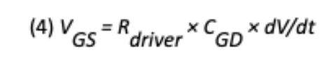
The capacitive dV/dt turn-on is strongly circuit dependent.
If the dV/dt across the MOSFETs drain to source is too high, it may charge CGD, which is the capacitance between drain and gate, inducing a voltage at the gate. The gate voltage depends on the pull-down resistor of the driver based on Equation (4).
In some bipolar drive circuits, such as emitter follower derived circuits, the problem is increased. It is because the driver cannot pull the gate down to 0 V and has approximately 0.7 V offset.
It is also important that the driver is referenced to the MOSFET source and not to signal ground, which can be significantly different in voltage.
The ratio of CGD to CGS is a factor but a good drive circuit is the critical factor.
Even if a VGS spike is present, it is safe for the MOSFET as long as the dissipation is within thermal limits and MOSFET SOA limits.
Nexperia MOSFETs are designed with a high threshold at high temperatures and we check VGS threshold at 25 °C is within data sheet limits. Logic level devices are designed and guaranteed to have a minimum threshold voltage >0.5 V even at 175 °C.
It is usually measured in a half-bridge test circuit. It is a measure of the device dV/dt during body diode reverse recovery. This data is not normally published in the data sheet. This dV/dt is in practice the highest dV/dt the device experiences.
High dV/dt can induce glitches onto the gate of the MOSFET. A snubber can help to reduce dV/dt and the magnitude of the VDS spike if significant. The ratio of Coss at low VDS compared to Coss value at high VDS is an indicator of the non-linearity of Coss. A very high ratio can indicate that the device can generate a high dV/dt. Gate driver circuit design can reduce the gate glitch. The ratio of QGD to QGS and the gate threshold voltage can be used to indicate the susceptibility of the device to gate glitches.
In theory, all MOSFETs are.
Soft recovery does reduce the dV/dt. Although dV/dt is not an issue for the MOSFET, a lower dV/dt is better for EMI, voltage spikes and crosstalk. The design and manufacture is very specialized, involving proprietary information.
At high temperatures, it is easier to trigger a parasitic bipolar as its VBE reduces. But if the BJT is effectively shorted out and current diverted away from it, then it is not an issue.
The aim is to obtain a dV/dt value to check if parasitic BJT turns on, leading to device failure. It is impossible to measure the characteristics of the parasitic bipolar transistor as its terminals cannot be accessed independently of the MOSFET terminals. A parasitic bipolar transistor is always created when a MOSFET is fabricated.
It is sometimes referred to as gate bounce. MOSFETs have internal stray capacitances coupling all three terminals and the gate is floating. The capacitors are inherent to the internal structure of a MOSFET.
CGD and CGS form a capacitive potential divider. When a voltage appears across the drain and source of the MOSFET, it couples to the gate and causes the internal gate source capacitor to charge. If the voltage on the gate increases beyond the MOSFET's threshold voltage, it starts to turn back on which can cause cross conduction. The ratio of the capacitances CGD and CGS determines the severity of this effect.
If improved thermal resistance is required, vias can be added to the footprint. The effect of adding vias is discussed in Section 3.5 of AN10874.
We do not perform any HV isolation tests on any automotive MOSFETs or specify any HV isolation parameter in our data sheets. Insulation testing is only applicable to TO-220F packages (Nexperia SOT186A)
Environmental conditions: 4-layer FR4 board at 105 °C ambient temperature.
Although it is possible to reduce efficiency, other factors become the constraints.
There is a strong similarity between the data sheet characteristics and the Nexperia SPICE models at 25 °C. It is especially true for transfer curve, RDS(on), diode characteristic, and gate charge. The SPICE model also accounts for the package parasitic resistances and inductances.
The SPICE models provided by Nexperia are generated from measurements performed on a sample of devices. Several parameters such as transfer characteristics, output characteristics
and gate charge are used. Values for parasitic package impedances and the data sheet maximum RDS(on) value are combined to produce a model that emulates the behavior of the sample MOSFETs.
- It is important to note that the SPICE models generated by Nexperia:
- represent typical parts that can be found within the production distribution.
- are set close to the maximum RDS(on) of the part without adversely affecting the other model parameters.
- are only valid for Tj = 25 °C.
Customers wishing to do design validation using a SPICE model, are advised to proceed with caution given the information provided above. Nexperia encourages designers to perform Monte Carlo simulations and use tolerance stacks in their simulation design. These factors permit part to part variation of their whole system to be accounted for.
Nexperia can advise on what reasonable levels of tolerance on key parameters for the MOSFET would be.
Drift engineering is optimizing of the drift region between the bottom of the trench and the epi/ substrate interface (light green area). The drift region supports most of the drain-source voltage in the off state. The purpose of drift engineering is to reduce the resistance of the drift region while maintaining the drain-source breakdown voltage V(BR)DSS capability.
Reduced cell pitch generally results in lower resistance and higher capacitance. The goal of each new generation of MOSFET technology is to reduce RDS(on) without a large increase in capacitance that usually accompanies reduced cell pitch. Reduced cell pitch also reduces SOA capability (linear mode operation) but improves avalanche capability.
Shorter channel gives a lower RDS(on) and a lower CGS capacitance simultaneously. It has higher leakage current and the transfer curve (ID versus VGS characteristic) becomes more dependent on VDS. It is also observed in the output characteristics.
Thick bottom oxide refers to gate oxide at the bottom of the trench. It is made thicker than the gate oxide at the side of the trench. It acts as a thicker dielectric between the gate and the drain resulting in a much lower CGD value.
Nexperia continues to supply older products where the volumes of manufacture are economically viable. The sales price margin is commercially viable and there are no manufacturing reasons which prevent manufacture.
A Discontinuation of Delivery (DoD) document notifies key customers (including distributors), when a part is planned to be withdrawn. It allows customers to make arrangements to buy sufficient products for future requirements and if necessary qualify alternative products.
We have a detailed application note on this subject, AN90011, please refer to this for any EMC related concerns.
The key parameters are the gate oxide breakdown voltage and the gate input capacitance (Ciss). JESD22-A114 specifies the ESD Human Body Model test arrangement and results assessment criteria.
This formula estimates the ESD capability:
Vesd (HBM) = 16 × VGS(max) × Ciss (nF)
Yes. The ESD rating relies upon Ciss and gate oxide breakdown voltage. As Nexperia improves technology and the levels of quality and reliability also improve new generations tend to have stronger gate oxides. However as we improve our switching figure of merit (QG × RDS(on)), now for the same RDS(on) new technologies will have lower Ciss and therefore lower ESD rating.
In order to effectively screen MOSFETs with weak gate oxide and achieve <1 ppm quality levels, Nexperia uses special test techniques which involve accurately measuring the gate-source leakage behavior. Adding ESD protection networks means that it becomes very difficult to measure the gate-source leakage characteristics of the gate oxide because the ESD protection network will have a significantly higher leakage current. This means we cannot screen out weaker oxides and will result in a higher field failure rates. Furthermore, adding protection networks results in higher production costs. ESD protection networks are therefore only used where necessary.
Generally, for larger MOSFETs with good gate oxide quality and relatively high Ciss there is no need for ESD protection, as long as these are being mounted onto a PCB in a controlled ESD environment. For special applications where the MOSFET would be subjected directly to ESD in a finished product such as a lithium ion battery module or a power or signal port then on-chip ESD protection may be required to meet IEC 61000-4-2 or other ESD test specifications. Some very small MOSFETs from Nexperia may require on chip ESD protection networks in order to allow handling (such as NX3008NBKW), even in well controlled manufacturing environments.
The fundamental relationship between drain leakage current and temperature is exponential in form. The data sheet gives maximum values of IDSS at Tj = 25 °C and 175 °C.
Although these two parameters reference the voltage rating of the part, they look at different characteristics of the product. Drain leakage current (IDSS) is the current which flows when VDS equal to the rated voltage is applied. The test checks that the current is below the limit.
The breakdown voltage of a device V(BR)DSS is the VDS required to cause a drain current of 250 μA to flow. In practice it is slightly higher than the rated voltage of the device and the actual voltage varies for the same nominal type due to manufacturing variations. The minimum V(BR)DSS stated in the data sheet is the rated voltage. Breakdown voltage looks at the characteristic of the part when it is in avalanche. The mechanisms causing leakage current and avalanche current are different.
Nexperia has a high degree of confidence that this scenario would be OK even in the worst case. However, it cannot be 100 % guaranteed by a production test at 25 °C.
The following principle could be applied to any Nexperia MOSFET technology at any breakdown voltage rating. In the data sheet, the values for minimum drain-source breakdown voltages are specified at -55 °C and 25 °C. The correlation between V(BR)DSS and temperature is approximately linear over this range. Therefore, a straight line can be plotted at Temperature (-55 °C and 25 °C) versus V(BR)DSS (at -55 °C and 25 °C).
For example: a 40 V Trench generation 6 part, has a V(BR)DSS at -55 °C of 36 V and 40 V at 25 °C. Using linear interpolation, gives a V(BR)DSS of 36.75 V at -40 °C.
The answer to this question is not simple - there are several factors which would affect the ID value.
Unfortunately, Nexperia cannot supply values for these capacitances at the extremes of the MOSFET operating temperature range requested. It is due to the limitations of our parametric test equipment. However, we can comment on how these capacitances vary with temperature and the MOSFET terminal voltages.
Ciss is the input capacitance formed by the parallel combination of CGS and CGD, and CGS dominates. CGS is formed across the gate oxide so it does not vary significantly with
temperature or the MOSFET terminal voltages. As CGS depends on gate oxide thickness and other defined die feature dimensions, it should not vary much between samples.
Crss is the reverse transfer capacitance which is essentially the gate-drain capacitance (CGD). It is formed across the MOSFET body diode depletion layer. This layer becomes thicker, as the reverse voltage (VDS) across it increases. Crss increases as VDS decreases. Crss has a greater variability than Ciss because it depends on the body diode depletion layer.
Coss is the output capacitance formed by the parallel combination of CDS and CGD. The drain- source capacitance (CDS) also dominates this capacitance. It varies with VDS in a similar way to Crss varying with VDS and it has similar variability to Crss for the same reasons.
It has been observed that switching losses only slightly increase at Tj(max), in the order of 10 %, since the capacitances only marginally change. Other factors can influence switching behavior, especially where the gate driver current capability changes significantly with temperature. The depletion layer thickness varies in proportion to the square root of the absolute temperature in K and it affects Crss and Coss.
Worst case values of minimum and maximum VGS(th) should be used for design purposes. They are given in the data sheet Characteristics.
The measured RG value is in the range of 1 Ω to 3 Ω and it does not vary significantly with temperature. In our general MOSFET characterization, it is presently not possible to test RG over the temperature range.
The minimum current that is expected at a VDS of 0.1 V can be calculated from the maximum (175 °C) RDS(on) value (26 mΩ).
The drain current that flows with these conditions is 0.1/0.026 = 3.846 A. The maximum die temperature is the critical factor. Do not allow it to exceed 175 °C.
However, if the RDS(on) is not at the top limit of the value range or the die temperature is lower, it is lower. As a result, the corresponding drain current is proportionately higher.
The maximum RDSon is 11.5 mΩ at Tmb = 25 °C. The maximum die temperature is likely to be higher than 25 °C in most applications.
If the mounting base temperature is maintained at 100 °C or less, the (fully ON) MOSFET can safely carry a continuous current up to 35 A.
The (fully ON) MOSFET can also sustain a current pulse of 204 A for a period up to 10 μs.
The ratings given on the data sheet are for each individual MOSFET in this device.
Although there are two MOSFETs housed within the package, they are fully electrically isolated from each other.
However, as the MOSFETs share a common package, there is a small amount of thermal coupling between the two MOSFET dies through the plastic package material. The heat generated by the power dissipated in one MOSFET increases the temperature of the other, even though the other may not be dissipating power. In an application, there is also an external thermal coupling path via the PCB to which the device is mounted. In practice, it is the main thermal coupling mechanism between the two dies.
To guarantee long-term reliability, it is very important that the junction temperature of either of the dies is never allowed to exceed 175 °C.
The individual MOSFET mounting bases are the main exit routes for heat generated in the dies. In practice, the mounting bases are soldered to copper pads on a Printed-Circuit Board (PCB). They provide the electrical connections to the MOSFET drains and heat sinking. Both MOSFETs in the package should operate at their rated power/current when their mounting bases are maintained at 25 °C. However, it is very difficult to achieve in practice and de-rating must be done in most cases.
Data from a T9 MOSFET family device BUK7J1R4-40H is considered but the principle can be applied to T6 devices also. The plateau voltage in the gate charge characteristic is the horizontal portion of the Gate-source voltage as a function of gate charge graph (see Fig 13. in datasheet); and is related to the transfer characteristic (Fig. 8).
The plateau voltage is around 4.25 V typical for a current of 25 A. This corresponds to the value in the transfer curve, also for a typical device. So at -55 °C then the plateau voltage will be 4.35 V and at 175 °C it will be 3.9 V for a typical device.
When considering a “worst case” device then the spread in gate threshold VGS(th) needs to be considered. It is assumed that the gain (transconductance) of the device is not affected by the same process related reasons which affect VGS(th). The transfer curve for a typical device would be shifted along the VGS axis according to the delta in the VGS(th).
The plateau voltage at the 25 A test condition would be 3.65 V for minimum VGS(th) and 4.85 V maximum VGS(th).
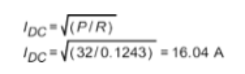
Consider a specific example such as BUK9K52-60E. See table 1 in the datasheet for capability.
The key point is the Ptot of 32 W. This is per die at data sheet conditions which assume that the mounting base is maintained at 25 °C. The maximum DC current allowed in each device would be
16.04 A, based on RDSon of 124.3 mΩ (VGS= 5 V) at 175 °C.
If both devices in the package are considered then the total power dissipation when both mounting bases are maintained at 25 °C is 32 W x 2 = 64 W. This only applies when the mounting bases of the devices are maintained at 25 °C (using an infinite heatsink). The power capability will decrease as the mounting base temperatures increase such that Tj does not exceed 175 °C. Consequently the current will decrease as shown in the Fig 2 in datasheet of ID vs Tmb, if the mounting base is maintained at a different temperature such as 125 °C, the current rating would be 9.26 A.
FIT (Failure In Time) is commonly used to express component reliability. It is defined as the number of failures occurring in 1 × 1000000000 hours (1 billion hours).
At any elapsed time (t), the reliability (R) of a group of operating semiconductors is: R(t) = (no - nf)/no
Where:
no is the original sample size and nf is the number of failures after time t.
Over the standard time of 10^9 hours, it approximates to F = (1/no)*(nf/t)*1000000000.