74AVC4T3144-Q100
Parametrics
| Type number | VCC (V) | Logic switching levels | Output drive capability (mA) | Nr of bits | Power dissipation considerations | Tamb (°C) | Rth(j-a) (K/W) | Ψth(j-top) (K/W) | Rth(j-c) (K/W) | Package name |
|---|---|---|---|---|---|---|---|---|---|---|
| 74AVC4T3144GU12-Q100 | n.a. | CMOS/LVTTL | ± 12 | 4 | very low | -40~125 | 188 | 6.2 | 96 | XQFN12 |
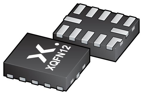
Package
| Type number | Orderable part number, (Ordering code (12NC)) | Status | Marking | Package | Package information | Reflow-/Wave soldering | Packing |
|---|---|---|---|---|---|---|---|
| 74AVC4T3144GU12-Q100 | 74AVC4T3144GU12-QX (935690912115) |
Active | Bd |
XQFN12 (SOT1174-1) |
SOT1174-1 | SOT1174-1_115 |
Environmental information
| Type number | Orderable part number | Chemical content | RoHS | RHF-indicator |
|---|---|---|---|---|
| 74AVC4T3144GU12-Q100 | 74AVC4T3144GU12-QX | 74AVC4T3144GU12-Q100 |
|
|
Documentation (8)
| File name | Title | Type | Date |
|---|---|---|---|
| 74AVC4T3144_Q100 | 4-bit dual-supply buffer/level translator; 3-state | Data sheet | 2024-07-02 |
| AN90007 | Pin FMEA for AVC family | Application note | 2018-11-30 |
| AN90063 | Questions about package outline drawings | Application note | 2025-06-13 |
| SOT1174-1 | 3D model for products with SOT1174-1 package | Design support | 2021-01-28 |
| avc4t3144 | IBIS model of 74AVC4T3144 | IBIS model | 2017-12-22 |
| 74AVC4T3144_and_74LVC4T3144_leaflet | Dual supply translating buffers/line drivers | Leaflet | 2018-03-09 |
| Nexperia_package_poster | Nexperia package poster | Leaflet | 2020-05-15 |
| SOT1174-1 | plastic, leadless extremely thin quad flat package; 12 terminals; 0.4 mm pitch; 2 mm x 1.7 mm x 0.5 mm body | Package information | 2024-04-11 |
Support
If you are in need of design/technical support, let us know and fill in the answer form we'll get back to you shortly.
Ordering, pricing & availability
Sample
As a Nexperia customer you can order samples via our sales organization.
If you do not have a direct account with Nexperia our network of global and regional distributors is available and equipped to support you with Nexperia samples. Check out the list of official distributors.