
74AUP1T97
Parametrics
| Type number | VCC (V) | Logic switching levels | Output drive capability (mA) | tpd (ns) | fmax (MHz) | Nr of bits | Power dissipation considerations | Tamb (°C) | Rth(j-a) (K/W) | Ψth(j-top) (K/W) | Rth(j-c) (K/W) | Package name |
|---|---|---|---|---|---|---|---|---|---|---|---|---|
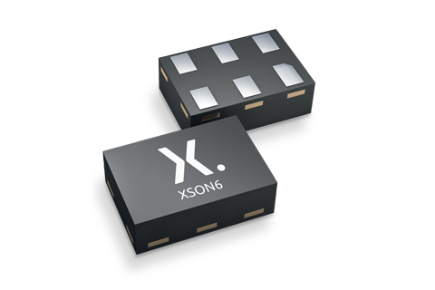
| 74AUP1T97GM | 2.3 - 3.6 | CMOS | ± 4 | 3.9 | 70 | 1 | ultra low | -40~125 | 290 | 6.5 | 145 | XSON6 |
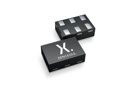
| 74AUP1T97GN | 2.3 - 3.6 | CMOS | ± 4 | 3.9 | 70 | 1 | ultra low | -40~125 | 275 | 11.7 | 171 | XSON6 |
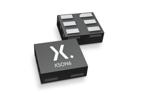
| 74AUP1T97GS | 2.3 - 3.6 | CMOS | ± 4 | 3.9 | 70 | 1 | ultra low | -40~125 | 272 | 14.8 | 177 | XSON6 |
| 74AUP1T97GW | 2.3 - 3.6 | CMOS | ± 4 | 3.9 | 70 | 1 | ultra low | -40~125 | 264 | 38.6 | 153 | TSSOP6 |
| 74AUP1T97GX | 2.3 - 3.6 | CMOS | ± 4 | 3.9 | 70 | 1 | ultra low | -40~125 | 316 | 85.8 | 186 | X2SON6 |
Package
| Type number | Orderable part number, (Ordering code (12NC)) | Status | Marking | Package | Package information | Reflow-/Wave soldering | Packing |
|---|---|---|---|---|---|---|---|
| 74AUP1T97GM | 74AUP1T97GM,115 (935280469115) |
Active | 59 |
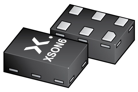
XSON6 (SOT886) |
SOT886 |
REFLOW_BG-BD-1
|
SOT886_115 |
| 74AUP1T97GM,132 (935280469132) |
Active | 59 | SOT886_132 | ||||
| 74AUP1T97GN | 74AUP1T97GN,132 (935288986132) |
Active | 59 |
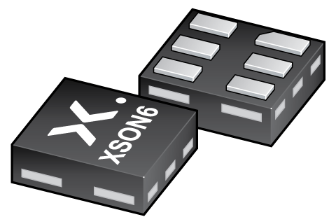
XSON6 (SOT1115) |
SOT1115 |
REFLOW_BG-BD-1
|
SOT1115_132 |
| 74AUP1T97GS | 74AUP1T97GS,132 (935292881132) |
Active | 59 |
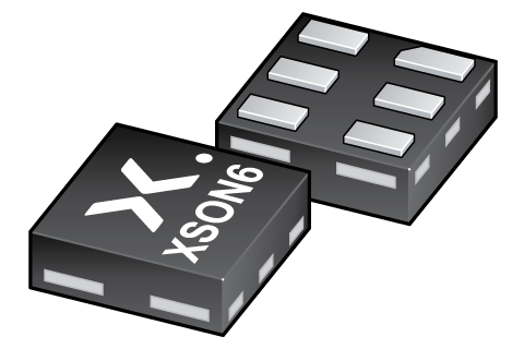
XSON6 (SOT1202) |
SOT1202 |
REFLOW_BG-BD-1
|
SOT1202_132 |
| 74AUP1T97GW | 74AUP1T97GW,125 (935280468125) |
Active | 59 |
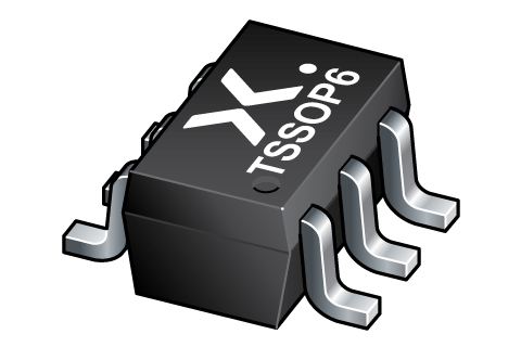
TSSOP6 (SOT363-2) |
SOT363-2 | SOT363-2_125 | |
| 74AUP1T97GX | 74AUP1T97GXZ (935307073147) |
Active | 59 |
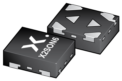
X2SON6 (SOT1255-2) |
SOT1255-2 | SOT1255-2_147 |
Environmental information
| Type number | Orderable part number | Chemical content | RoHS | RHF-indicator |
|---|---|---|---|---|
| 74AUP1T97GM | 74AUP1T97GM,115 | 74AUP1T97GM |
|
|
| 74AUP1T97GM | 74AUP1T97GM,132 | 74AUP1T97GM |
|
|
| 74AUP1T97GN | 74AUP1T97GN,132 | 74AUP1T97GN |
|
|
| 74AUP1T97GS | 74AUP1T97GS,132 | 74AUP1T97GS |
|
|
| 74AUP1T97GW | 74AUP1T97GW,125 | 74AUP1T97GW |
|
|
| 74AUP1T97GX | 74AUP1T97GXZ | 74AUP1T97GX |
|
|
Documentation (28)
| File name | Title | Type | Date |
|---|---|---|---|
| AN90063 | Questions about package outline drawings | Application note | 2025-03-12 |
| Nexperia_document_guide_Logic_translators | Nexperia Logic Translators | Brochure | 2021-04-12 |
| Nexperia_document_guide_MiniLogic_MicroPak_201808 | MicroPak leadless logic portfolio guide | Brochure | 2018-09-03 |
| SOT891 | 3D model for products with SOT891 package | Design support | 2019-10-03 |
| SOT886 | 3D model for products with SOT886 package | Design support | 2019-10-03 |
| SOT1115 | 3D model for products with SOT1115 package | Design support | 2023-02-02 |
| SOT1202 | 3D model for products with SOT1202 package | Design support | 2023-02-02 |
| SOT363-2 | 3D model for products with SOT363-2 package | Design support | 2023-02-02 |
| SOT1255-2 | 3D model for products with SOT1255-2 package | Design support | 2021-01-28 |
| Nexperia_document_leaflet_Logic_AUP_technology_portfolio_201904 | Nexperia_document_leaflet_Logic_AUP_technology_portfolio_201904 | Leaflet | 2019-04-12 |
| Nexperia_document_leaflet_Logic_X2SON_packages_062018 | X2SON ultra-small 4, 5, 6 & 8-pin leadless packages | Leaflet | 2018-06-05 |
| Nexperia_package_poster | Nexperia package poster | Leaflet | 2020-05-15 |
| DFN1010-6_SOT891_mk | plastic, extremely thin small outline package; 6 terminals; 0.55 mm pitch; 1 mm x 1 mm x 0.5 mm body | Marcom graphics | 2017-01-28 |
| DFN1410-6_SOT886_mk | plastic, extremely thin small outline package; no leads; 6 terminals; 0.6 mm pitch; 1 mm x 1.45 mm x 0.5 mm body | Marcom graphics | 2017-01-28 |
| XSON6_SOT886_mk | plastic, extremely thin small outline package; no leads; 6 terminals; 0.6 mm pitch; 1 mm x 1.45 mm x 0.5 mm body | Marcom graphics | 2017-01-28 |
| XSON6_SOT1115_mk | plastic, extremely thin small outline package; 6 terminals; 0.55 mm pitch; 0.9 mm x 1 mm x 0.35 mm body | Marcom graphics | 2017-01-28 |
| SOT891 | plastic, leadless extremely thin small outline package; 6 terminals; 0.35 mm pitch; 1 mm x 1 mm x 0.5 mm body | Package information | 2020-04-21 |
| SOT886 | plastic, leadless extremely thin small outline package; 6 terminals; 0.5 mm pitch; 1 mm x 1.45 mm x 0.5 mm body | Package information | 2022-06-01 |
| SOT1115 | plastic, leadless extremely thin small outline package; 6 terminals; 0.3 mm pitch; 0.9 mm x 1 mm x 0.35 mm body | Package information | 2022-05-27 |
| SOT1202 | plastic, leadless extremely thin small outline package; 6 terminals; 0.35 mm pitch; 1 mm x 1mm x 0.35 mm body | Package information | 2022-06-01 |
| SOT363-2 | plastic thin shrink small outline package; 6 leads; body width 1.25 mm | Package information | 2022-11-21 |
| SOT1255-2 | plastic thermal enhanced extremely thin small outline package; no leads;6 terminals; body 1.0 x 0.8 x 0.32 mm | Package information | 2020-08-27 |
| REFLOW_BG-BD-1 | Reflow soldering profile | Reflow soldering | 2021-04-06 |
| Nexperia_Selection_guide_2023 | Nexperia Selection Guide 2023 | Selection guide | 2023-05-10 |
| MAR_SOT891 | MAR_SOT891 Topmark | Top marking | 2013-06-03 |
| MAR_SOT886 | MAR_SOT886 Topmark | Top marking | 2013-06-03 |
| MAR_SOT1115 | MAR_SOT1115 Topmark | Top marking | 2013-06-03 |
| MAR_SOT1202 | MAR_SOT1202 Topmark | Top marking | 2013-06-03 |
Support
If you are in need of design/technical support, let us know and fill in the answer form we'll get back to you shortly.
Models
| File name | Title | Type | Date |
|---|---|---|---|
| SOT891 | 3D model for products with SOT891 package | Design support | 2019-10-03 |
| SOT886 | 3D model for products with SOT886 package | Design support | 2019-10-03 |
| SOT1115 | 3D model for products with SOT1115 package | Design support | 2023-02-02 |
| SOT1202 | 3D model for products with SOT1202 package | Design support | 2023-02-02 |
| SOT363-2 | 3D model for products with SOT363-2 package | Design support | 2023-02-02 |
| SOT1255-2 | 3D model for products with SOT1255-2 package | Design support | 2021-01-28 |
Ordering, pricing & availability
Sample
As a Nexperia customer you can order samples via our sales organization.
If you do not have a direct account with Nexperia our network of global and regional distributors is available and equipped to support you with Nexperia samples. Check out the list of official distributors.