


Features and benefits
- Single N-Channel
- Ultra small silicon (wafer level) package: 1 × 0.6 × 0.2 mm
- Best in class RDS(on) performance (50 mΩ)
- Lowest RDS(on) per mm² in 30 V
- Offerings with and without 2 KV HBM ESD protection
- ID up to 4 A
- Low voltage drive (VGS(th) = 0.8 V typ.)
- VDS = 30V; VGS = 12 V
Applications
- Standard switch for portables/wearables where space is key - hearing aids, earphones, smart watches
- Battery management
- Low-side load switch
- Relay driver
Featured documents
Latest news and blogs

Documentation
| File name | Title | Type | Date |
|---|---|---|---|
| AN90017.pdf | Load switches for mobile and computing applications | Application note | 2020-09-02 |
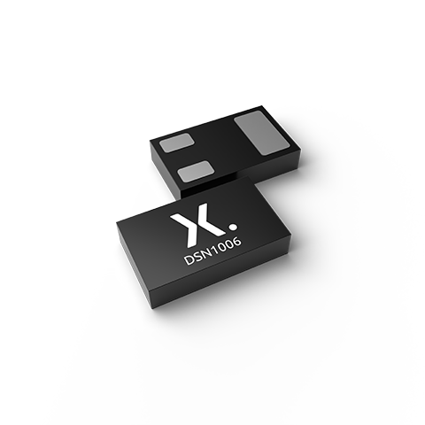
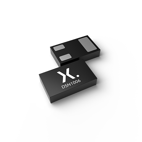
| sot8026_3d.png | DSN1006-3; chip-scale package; 3 terminals; body 1 x 0.6 x 0.2 mm | Outline 3d | 2021-07-19 |
| vp_DSN1006_MOSFETs.zip | DSN1006 MOSFETs | Value proposition | 2022-05-26 |
| RS3885_DSN1006-SOT8026_Combi.png | DSN1006 (SOT8026) MARCOM image | Marcom graphics | 2022-06-06 |
| nexperia_document_leaflet_SsMOS_for_mobile_2022-CHN.pdf | 适合移动和便携式设备的 大批量小信号MOSFET, 采用WLCSP和无引脚DFN封装 | Leaflet | 2022-07-04 |
| nexperia_document_leaflet_SsMOS_for_mobile_2022.pdf | High volume small-signal MOSFETs for mobile and portables, in WLCSP and leadless DFN packages | Leaflet | 2022-07-04 |
| AN90036.pdf | Recommendations for Printed Circuit Board assembly of DSN1006-3 (SOT8026) | Application note | 2022-08-09 |
| SOT8026.pdf | chip-scale package; 3 terminals; body 1.0 x 0.6 x 0.2 mm | Package information | 2023-02-28 |
| AN11304.pdf | MOSFET load switch PCB with thermal measurement | Application note | 2025-10-21 |
| AN90009.pdf | Leakage of small-signal MOSFETs | Application note | 2025-10-21 |
Please contact us if you have any questions. If you are in need of design support, please fill in the answer form, we will get back to you shortly.
Please visit our contact us or {1} for further support.