
74LV08-Q100
Parametrics
| Type number | VCC (V) | Logic switching levels | Output drive capability (mA) | tpd (ns) | fmax (MHz) | Nr of bits | Power dissipation considerations | Tamb (°C) | Rth(j-a) (K/W) | Ψth(j-top) (K/W) | Rth(j-c) (K/W) | Package name |
|---|---|---|---|---|---|---|---|---|---|---|---|---|
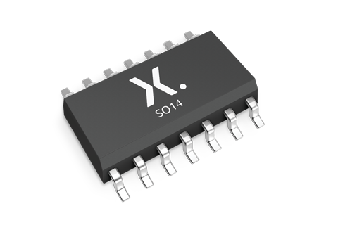
| 74LV08D-Q100 | 1.0 - 5.5 | TTL | ± 12 | 7 | 30 | 4 | low | -40~125 | 87 | 6.6 | 45 | SO14 |
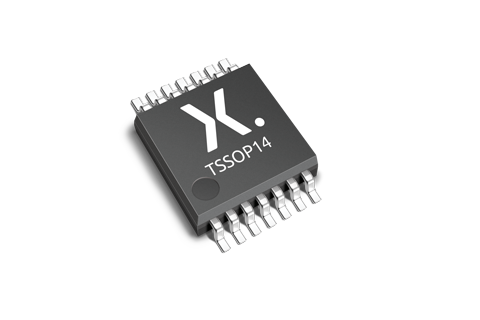
| 74LV08PW-Q100 | 1.0 - 5.5 | TTL | ± 12 | 7 | 30 | 4 | low | -40~125 | 127 | 3.1 | 51.4 | TSSOP14 |
Package
| Type number | Orderable part number, (Ordering code (12NC)) | Status | Marking | Package | Package information | Reflow-/Wave soldering | Packing |
|---|---|---|---|---|---|---|---|
| 74LV08D-Q100 | 74LV08D-Q100,118 (935299069118) |
Active | 74LV08D |
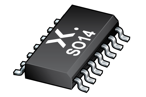
SO14 (SOT108-1) |
SOT108-1 |
SO-SOJ-REFLOW
SO-SOJ-WAVE WAVE_BG-BD-1 |
SOT108-1_118 |
| 74LV08PW-Q100 | 74LV08PW-Q100,118 (935299071118) |
Active | LV08 |
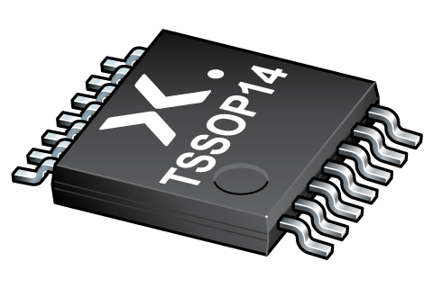
TSSOP14 (SOT402-1) |
SOT402-1 |
SSOP-TSSOP-VSO-WAVE
|
SOT402-1_118 |
Environmental information
| Type number | Orderable part number | Chemical content | RoHS | RHF-indicator |
|---|---|---|---|---|
| 74LV08D-Q100 | 74LV08D-Q100,118 | 74LV08D-Q100 |
|
|
| 74LV08PW-Q100 | 74LV08PW-Q100,118 | 74LV08PW-Q100 |
|
|
Documentation (16)
| File name | Title | Type | Date |
|---|---|---|---|
| 74LV08_Q100 | Quad 2-input AND gate | Data sheet | 2024-01-30 |
| AN90063 | Questions about package outline drawings | Application note | 2025-03-12 |
| mna221 | Block diagram: 74AHC08BQ, 74AHC08D, 74AHC08PW, 74AHC2G08DC, 74AHC2G08DP, 74AHC2G08GD, 74AHCT08BQ, 74AHCT08D, 74AHCT08PW, 74AHCT2G08DC, 74AHCT2G08DP, 74AHCT2G08GD, 74AUP1G08GF, 74AUP1G08GM, 74AUP1G08GW, 74HC2G08DC, 74HC2G08DP, 74HC2G08GD, 74HCT2G08DC, 74HCT2G08DP, 74HCT2G08GD, 74LV08D, 74LV08DB, 74LV08N, 74LV08PW, 74LV125D, 74LV125DB, 74LV125N, 74LV125PW | Block diagram | 2009-11-03 |
| SOT108-1 | 3D model for products with SOT108-1 package | Design support | 2020-01-22 |
| SOT402-1 | 3D model for products with SOT402-1 package | Design support | 2023-02-02 |
| 74lv08 | 74lv08 IBIS model | IBIS model | 2016-05-25 |
| Nexperia_package_poster | Nexperia package poster | Leaflet | 2020-05-15 |
| SO14_SOT108-1_mk | plastic, small outline package; 14 leads; 1.27 mm pitch; 8.65 mm x 3.9 mm x 1.75 mm body | Marcom graphics | 2017-01-28 |
| TSSOP14_SOT402-1_mk | plastic, thin shrink small outline package; 14 leads; 0.65 mm pitch; 5 mm x 4.4 mm x 1.1 mm body | Marcom graphics | 2017-01-28 |
| SOT108-1 | plastic, small outline package; 14 leads; 1.27 mm pitch; 8.65 mm x 3.9 mm x 1.75 mm body | Package information | 2023-11-07 |
| SOT402-1 | plastic, thin shrink small outline package; 14 leads; 0.65 mm pitch; 5 mm x 4.4 mm x 1.2 mm body | Package information | 2023-11-07 |
| SO-SOJ-REFLOW | Footprint for reflow soldering | Reflow soldering | 2009-10-08 |
| Nexperia_Selection_guide_2023 | Nexperia Selection Guide 2023 | Selection guide | 2023-05-10 |
| SO-SOJ-WAVE | Footprint for wave soldering | Wave soldering | 2009-10-08 |
| WAVE_BG-BD-1 | Wave soldering profile | Wave soldering | 2021-09-08 |
| SSOP-TSSOP-VSO-WAVE | Footprint for wave soldering | Wave soldering | 2009-10-08 |
Support
If you are in need of design/technical support, let us know and fill in the answer form we'll get back to you shortly.
Ordering, pricing & availability
Sample
As a Nexperia customer you can order samples via our sales organization.
If you do not have a direct account with Nexperia our network of global and regional distributors is available and equipped to support you with Nexperia samples. Check out the list of official distributors.