Orderable parts
| Type number | Orderable part number | Ordering code (12NC) | Package | Buy from distributors |
|---|---|---|---|---|
| 74ALVCH16823DGG | 74ALVCH16823DGG,11 | 935259030118 | SOT364-1 | Order product |
Discover Nexperia’s extensive portfolio of diodes, bipolar transistors, ESD protection devices, MOSFETs, GaN FETs, IGBTs, and analog & logic ICs. Our components power virtually every electronic design worldwide - from automotive and industrial to mobile and consumer applications.
Our products find applications across various industries, from automotive and industrial to power, computing, consumer, mobile, and wearables. With a commitment to innovation and sustainability, our components set benchmarks in efficiency, empowering our global customer base to develop energy-efficient and cutting-edge solutions.
Try out our devices and their performance with our comprehensive range of evaluation boards. Gain a deeper understanding of how our products can benefit your application, whether it's optimizing for efficiency, robustness, or reliability. You can find Application focus, Package focus, and different Nexperia Product focus boards here.
Register once, drag and drop ECAD models into your CAD tool and speed up your design.
Click here for more information18-bit bus-interface D-type flip-flop with reset and enable; 3-state
The 74ALVCH16823 is an 18-bit edge-triggered flip-flop featuring separate D-type inputs for each flip-flop and 3-state outputs for bus oriented applications. Incorporates bushold data inputs which eliminate the need for external pull-up resistors to hold unused inputs. The 74ALVCH16823 consists of two sections of nine edge-triggered flip-flops. A clock (nCP) input, an output-enable (nOE) input, a master reset (nMR) input and a clock-enable (nCE) input are provided for each total 9-bit section.
With the clock-enable (nCE) input LOW, the D-type flip-flops will store the state of their individual nDn-inputs that meet the set-up and hold time requirements on the LOW-to-HIGH nCP transition. Taking nCE HIGH disables the clock buffer, thus latching the outputs. Taking the master reset (nMR) input LOW causes all the nQn outputs to go LOW independently of the clock.
When nOE is LOW, the contents of the flip-flops are available at the outputs. When the nOE is HIGH, the outputs go to the high impedance OFF-state. Operation of the nOE input does not affect the state of flip-flops.
Active bus hold circuitry is provided to hold unused or floating data inputs at a valid logic level.
Wide supply voltage range from 1.2 V to 3.6 V
CMOS low-power consumption
Direct interface with TTL levels
Current drive ± 24 mA at 3.0 V
MULTIBYTE™ flow-through standard pin-out architecture
Low inductance multiple VCC and GND pins for minimum noise and ground bounce
Output drive capability 50 Ω transmission lines at 85°C
All data inputs have bushold
Complies with JEDEC standard no. 8-1A
Complies with JEDEC standards:
JESD8-5 (2.3 V to 2.7 V)
JESD8B/JESD36 (2.7 V to 3.6 V)
ESD protection:
| Type number | VCC (V) | Logic switching levels | Output drive capability (mA) | tpd (ns) | fmax (MHz) | Power dissipation considerations | Tamb (°C) | Rth(j-a) (K/W) | Ψth(j-top) (K/W) | Package name |
|---|---|---|---|---|---|---|---|---|---|---|
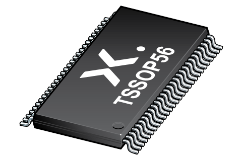
| 74ALVCH16823DGG | 1.2 - 3.6 | TTL | ± 24 | 2.1 | 350 | low | -40~85 | 93 | 21 | TSSOP56 |
| Type number | Orderable part number, (Ordering code (12NC)) | Status | Marking | Package | Package information | Reflow-/Wave soldering | Packing |
|---|---|---|---|---|---|---|---|
| 74ALVCH16823DGG | 74ALVCH16823DGG,11 (935259030118) |
Active | ALVCH16823 |
TSSOP56 (SOT364-1) |
SOT364-1 |
SSOP-TSSOP-VSO-WAVE
|
SOT364-1_118 |
All type numbers in the table below are discontinued.
| Type number | Orderable part number, (Ordering code (12NC)) | Status | Marking | Package | Package information | Reflow-/Wave soldering | Packing |
|---|---|---|---|---|---|---|---|
| 74ALVCH16823DGG | 74ALVCH16823DGGS (935259030512) |
Withdrawn / End-of-life | ALVCH16823 |
TSSOP56 (SOT364-1) |
SOT364-1 |
SSOP-TSSOP-VSO-WAVE
|
Not available |
| Type number | Orderable part number | Chemical content | RoHS | RHF-indicator |
|---|---|---|---|---|
| 74ALVCH16823DGG | 74ALVCH16823DGG,11 | 74ALVCH16823DGG |
|
|
All type numbers in the table below are discontinued.
| Type number | Orderable part number | Chemical content | RoHS | RHF-indicator |
|---|---|---|---|---|
| 74ALVCH16823DGG | 74ALVCH16823DGGS | 74ALVCH16823DGG |
|
|
| File name | Title | Type | Date |
|---|---|---|---|
| 74ALVCH16823 | 18-bit bus-interface D-type flip-flop with reset and enable; 3-state | Data sheet | 2024-07-09 |
| AN90063 | Questions about package outline drawings | Application note | 2025-06-13 |
| SOT364-1 | 3D model for products with SOT364-1 package | Design support | 2020-01-22 |
| alvch16823 | alvch16823 IBIS model | IBIS model | 2013-04-08 |
| Nexperia_package_poster | Nexperia package poster | Leaflet | 2020-05-15 |
| SOT364-1 | plastic, thin shrink small outline package; 56 leads; 0.5 mm pitch; 14 mm x 6.1 mm x 1.2 mm body | Package information | 2022-06-23 |
| SOT364-1_118 | TSSOP56; Reel pack for SMD, 13"; Q1/T1 product orientation | Packing information | 2020-04-21 |
| 74ALVCH16823DGG_Nexperia_Product_Reliability | 74ALVCH16823DGG Nexperia Product Reliability | Quality document | 2025-03-20 |
| SSOP-TSSOP-VSO-WAVE | Footprint for wave soldering | Wave soldering | 2009-10-08 |
If you are in need of design/technical support, let us know and fill in the answer form we'll get back to you shortly.
The Nexperia Longevity Program is aimed to provide our customers information from time to time about the expected time that our products can be ordered. The NLP is reviewed and updated regularly by our Executive Management Team. View our longevity program here.
| File name | Title | Type | Date |
|---|---|---|---|
| alvch16823 | alvch16823 IBIS model | IBIS model | 2013-04-08 |
| SOT364-1 | 3D model for products with SOT364-1 package | Design support | 2020-01-22 |
| Type number | Orderable part number | Ordering code (12NC) | Status | Packing | Packing Quantity | Buy online |
|---|---|---|---|---|---|---|
| 74ALVCH16823DGG | 74ALVCH16823DGG,11 | 935259030118 | Active | SOT364-1_118 | 2,000 |
|
As a Nexperia customer you can order samples via our sales organization.
If you do not have a direct account with Nexperia our network of global and regional distributors is available and equipped to support you with Nexperia samples. Check out the list of official distributors.
The interactive datasheets are based on the Nexperia MOSFET precision electrothermal models. With our interactive datasheets you can simply specify your own conditions interactively. Start by changing the values of the conditions. You can do this by using the sliders in the condition fields. By dragging the sliders you will see how the MOSFET will perform at the new conditions set.