Register once, drag and drop ECAD models into your CAD tool and speed up your design.
Click here for more information74ALVT16823DL
18-bit bus-interface D-type flip-flop with reset and enable; 3-state
The 74ALVT16823 is an 18-bit positive-edge triggered D-type flip-flop with 3-state outputs, reset and enable.
The device can be used as two 9-bit flip-flops or one 18-bit flip-flop. The device features clock (nCP), clock enable (nCE), master reset (nMR) and output enable (nOE, inputs each controlling 9-bits. When nCE is LOW, the flip-flops will store the state of their individual D-inputs that meet the set-up and hold time requirements on the LOW-to-HIGH clock (nCP) transition. A HIGH on nOE causes the outputs to assume a high-impedance OFF-state. Operation of the nOE input does not affect the state of the flip-flops. A LOW on nMR will reset the flip-flops LOW. Bus hold data inputs eliminate the need for external pull-up resistors to define unused inputs
Features and benefits
Wide supply voltage range from 2.3 V to 3.6 V
Overvoltage tolerant inputs to 5.5 V
BiCMOS high speed and output drive
Direct interface with TTL levels
Bus hold on data inputs
Power-up 3-state
IOFF circuitry provides partial Power-down mode operation
Two sets of high speed parallel registers with positive edge-triggered D-type flip-flops
Ideal where high speed, light loading, or increased fan-in are required with MOS microprocessors
Live insertion and extraction permitted
Power-up reset
No bus current loading when output is tied to 5 V bus
Output capability: +64 mA to -32 mA
Latch-up performance exceeds 500 mA per JESD 78 Class II Level B
ESD protection:
HBM: ANSI/ESDA/JEDEC JS-001 class 2 exceeds 2000 V
CDM: ANSI/ESDA/JEDEC JS-002 class C3 exceeds 1000 V
Specified from -40 °C to 85 °C
Parametrics
| Type number | Package name |
|---|---|
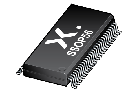
| 74ALVT16823DL | SSOP56 |
PCB Symbol, Footprint and 3D Model
| Model Name | Description |
|---|---|
|
|
Package
All type numbers in the table below are discontinued.
| Type number | Orderable part number, (Ordering code (12NC)) | Status | Marking | Package | Package information | Reflow-/Wave soldering | Packing |
|---|---|---|---|---|---|---|---|
| 74ALVT16823DL | 74ALVT16823DL,112 (935261020112) |
Obsolete | ALVT16823 |
SSOP56 (SOT371-1) |
SOT371-1 |
SSOP-TSSOP-VSO-REFLOW
SSOP-TSSOP-VSO-WAVE |
Not available |
| 74ALVT16823DL,118 (935261020118) |
Obsolete | ALVT16823 | Not available | ||||
| 74ALVT16823DL,512 (935261020512) |
Obsolete | ALVT16823 | Not available | ||||
| 74ALVT16823DL,518 (935261020518) |
Obsolete | ALVT16823 | Not available |
Environmental information
All type numbers in the table below are discontinued.
| Type number | Orderable part number | Chemical content | RoHS | RHF-indicator |
|---|---|---|---|---|
| 74ALVT16823DL | 74ALVT16823DL,112 | 74ALVT16823DL |
|
|
| 74ALVT16823DL | 74ALVT16823DL,118 | 74ALVT16823DL |
|
|
| 74ALVT16823DL | 74ALVT16823DL,512 | 74ALVT16823DL |
|
|
| 74ALVT16823DL | 74ALVT16823DL,518 | 74ALVT16823DL |
|
|
Series
Documentation (8)
| File name | Title | Type | Date |
|---|---|---|---|
| 74ALVT16823 | 18-bit bus-interface D-type flip-flop with reset and enable; 3-state | Data sheet | 2024-06-25 |
| AN90063 | Questions about package outline drawings | Application note | 2025-06-13 |
| alvt16823 | alvt16823 IBIS model | IBIS model | 2013-04-08 |
| Nexperia_package_poster | Nexperia package poster | Leaflet | 2020-05-15 |
| SOT371-1 | plastic, shrink small outline package; 56 leads; 0.635 mm pitch; 18.45 mm x 7.5 mm x 2.8 mm body | Package information | 2020-04-21 |
| SSOP-TSSOP-VSO-REFLOW | Footprint for reflow soldering | Reflow soldering | 2009-10-08 |
| alvt16 | alvt16 Spice model | SPICE model | 2013-05-07 |
| SSOP-TSSOP-VSO-WAVE | Footprint for wave soldering | Wave soldering | 2009-10-08 |
Support
If you are in need of design/technical support, let us know and fill in the answer form we'll get back to you shortly.
Longevity
The Nexperia Longevity Program is aimed to provide our customers information from time to time about the expected time that our products can be ordered. The NLP is reviewed and updated regularly by our Executive Management Team. View our longevity program here.
PCB Symbol, Footprint and 3D Model
| Model Name | Description |
|---|---|
|
|
How does it work?
The interactive datasheets are based on the Nexperia MOSFET precision electrothermal models. With our interactive datasheets you can simply specify your own conditions interactively. Start by changing the values of the conditions. You can do this by using the sliders in the condition fields. By dragging the sliders you will see how the MOSFET will perform at the new conditions set.