Register once, drag and drop ECAD models into your CAD tool and speed up your design.
Click here for more information74LVC823APW
9-bit D-type flip-flop with 5 V tolerant inputs/outputs; positive edge-trigger; 3-state
The 74LVC823A is a 9-bit D-type flip-flop with common clock (pin CP), clock enable (pin CE), master reset (pin MR) and 3-state outputs (pins Qn) for bus-oriented applications. The 9 flip-flops stores the state of their individual D-inputs that meet the set-up and hold times requirements on the LOW to HIGH CP transition, provided pin CE is LOW. When pin CE is HIGH, the flip-flops hold their data. A LOW on pin MR resets all flip-flops. When pin OE is LOW, the contents of the 9 flip-flops are available at the outputs. When pin OE is HIGH, the outputs go to the high-impedance OFF-state. Operation of the OE input does not affect the state of the flip-flops.
Inputs can be driven from either 3.3 V or 5 V devices. When disabled, up to 5.5 V can be applied to the outputs. These features allow the use of these devices as translators in mixed 3.3 V and 5 V applications.
Features and benefits
- 5 V tolerant inputs/outputs for interfacing with 5 V logic
- Wide supply voltage range from 1.2 V to 3.6 V
- CMOS low power consumption
- Direct interface with TTL levels
- Flow-through pinout architecture
- 9-bit positive edge-triggered register
- Independent register and 3-state buffer operation
- Complies with JEDEC standard:
- JESD8-7A (1.65 V to 1.95 V)
- JESD8-5A (2.3 V to 2.7 V)
- JESD8-C/JESD36 (2.7 V to 3.6 V)
- ESD protection:
- HBM JESD22-A114F exceeds 2000 V
- MM JESD22-A115-B exceeds 200 V
- CDM JESD22-C101E exceeds 1000 V
- Specified from -40 °C to +85 °C and -40 °C to +125 °C.
Parametrics
| Type number | Package name |
|---|---|
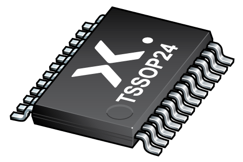
| 74LVC823APW | TSSOP24 |
PCB Symbol, Footprint and 3D Model
| Model Name | Description |
|---|---|
|
|
Package
All type numbers in the table below are discontinued.
| Type number | Orderable part number, (Ordering code (12NC)) | Status | Marking | Package | Package information | Reflow-/Wave soldering | Packing |
|---|---|---|---|---|---|---|---|
| 74LVC823APW | 74LVC823APW,112 (935262541112) |
Obsolete | LVC823A |
TSSOP24 (SOT355-1) |
SOT355-1 |
SSOP-TSSOP-VSO-WAVE
|
Not available |
| 74LVC823APW,118 (935262541118) |
Obsolete | LVC823A | SOT355-1_118 |
Environmental information
All type numbers in the table below are discontinued.
| Type number | Orderable part number | Chemical content | RoHS | RHF-indicator |
|---|---|---|---|---|
| 74LVC823APW | 74LVC823APW,112 | 74LVC823APW |
|
|
| 74LVC823APW | 74LVC823APW,118 | 74LVC823APW |
|
|
Documentation (10)
| File name | Title | Type | Date |
|---|---|---|---|
| 74LVC823A | 9-bit D-type flip-flop with 5 V tolerant inputs/outputs; positive edge-trigger; 3-state | Data sheet | 2020-06-19 |
| AN11009 | Pin FMEA for LVC family | Application note | 2019-01-09 |
| AN263 | Power considerations when using CMOS and BiCMOS logic devices | Application note | 2023-02-07 |
| AN90063 | Questions about package outline drawings | Application note | 2025-06-13 |
| SOT355-1 | 3D model for products with SOT355-1 package | Design support | 2020-01-22 |
| lvc823a | lvc823a IBIS model | IBIS model | 2013-04-09 |
| Nexperia_package_poster | Nexperia package poster | Leaflet | 2020-05-15 |
| SOT355-1 | plastic, thin shrink small outline package; 24 leads; 0.65 mm pitch; 7.8 mm x 4.4 mm x 1.2 mm body | Package information | 2024-11-15 |
| lvc | lvc Spice model | SPICE model | 2013-05-07 |
| SSOP-TSSOP-VSO-WAVE | Footprint for wave soldering | Wave soldering | 2009-10-08 |
Support
If you are in need of design/technical support, let us know and fill in the answer form we'll get back to you shortly.
Longevity
The Nexperia Longevity Program is aimed to provide our customers information from time to time about the expected time that our products can be ordered. The NLP is reviewed and updated regularly by our Executive Management Team. View our longevity program here.
PCB Symbol, Footprint and 3D Model
| Model Name | Description |
|---|---|
|
|
How does it work?
The interactive datasheets are based on the Nexperia MOSFET precision electrothermal models. With our interactive datasheets you can simply specify your own conditions interactively. Start by changing the values of the conditions. You can do this by using the sliders in the condition fields. By dragging the sliders you will see how the MOSFET will perform at the new conditions set.