Orderable parts
| Type number | Orderable part number | Ordering code (12NC) | Package | Buy from distributors |
|---|---|---|---|---|
| 74LVCH162374ADGG | 74LVCH162374ADGG:1 | 935238770118 | SOT362-1 | Order product |
Discover Nexperia’s extensive portfolio of diodes, bipolar transistors, ESD protection devices, MOSFETs, GaN FETs, IGBTs, and analog & logic ICs. Our components power virtually every electronic design worldwide - from automotive and industrial to mobile and consumer applications.
Our products find applications across various industries, from automotive and industrial to power, computing, consumer, mobile, and wearables. With a commitment to innovation and sustainability, our components set benchmarks in efficiency, empowering our global customer base to develop energy-efficient and cutting-edge solutions.
Try out our devices and their performance with our comprehensive range of evaluation boards. Gain a deeper understanding of how our products can benefit your application, whether it's optimizing for efficiency, robustness, or reliability. You can find Application focus, Package focus, and different Nexperia Product focus boards here.
Register once, drag and drop ECAD models into your CAD tool and speed up your design.
Click here for more information16-bit edge-triggered D-type flip-flop with 30 Ohm series termination resistors; 5 V input/output tolerant; 3-state
The 74LVCH162374A is a 16-bit edge triggered flip-flop featuring separate D-type inputs for each flip-flop and 3-state outputs for bus-oriented applications. The device consists of two sections of 8 edge-triggered flip-flops. A clock (CP) input and an output enable (OE) are provided for each octal. Inputs can be driven from either 3.3 V or 5 V devices. When disabled, up to 5.5 V can be applied to the outputs. These features allow the use of these devices in mixed 3.3 V and 5 V applications. The flip-flops store the state of their individual D-inputs that meet the set-up and hold time requirements on the LOW to HIGH CP transition. When OE is LOW, the contents of the flip-flops are available at the outputs. When OE is HIGH, the outputs go to the high-impedance OFF-state. Operation of the OE input does not affect the state of the flip-flops.
Bus hold on data inputs eliminates the need for external pull-up resistors to hold unused inputs.
To reduce line noise, 30 Ω series termination resistors are included in both high and low output stages.
5 V tolerant inputs/outputs for interfacing with 5 V logic
Wide supply voltage range from 1.2 V to 3.6 V
CMOS low power consumption
Multibyte flow-through standard pinout architecture
Multiple low inductance supply pins for minimum noise and ground bounce
Direct interface with TTL levels
All data inputs have bus hold
High-impedance outputs when VCC = 0 V
Complies with JEDEC standard:
JESD8-7A (1.65 V to 1.95 V)
JESD8-5A (2.3 V to 2.7 V)
JESD8-C/JESD36 (2.7 V to 3.6 V)
ESD protection:
HBM: ANSI/ESDA/JEDEC JS-001 class 2 exceeds 2000 V
CDM: ANSI/ESDA/JEDEC JS-002 class C3 exceeds 1000 V
Specified from -40 °C to +85 °C and -40 °C to +125 °C
| Type number | VCC (V) | Logic switching levels | Output drive capability (mA) | tpd (ns) | fmax (MHz) | Power dissipation considerations | Tamb (°C) | Rth(j-a) (K/W) | Ψth(j-top) (K/W) | Rth(j-c) (K/W) | Package name |
|---|---|---|---|---|---|---|---|---|---|---|---|
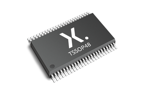
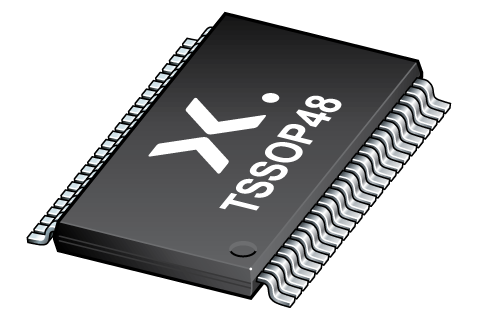
| 74LVCH162374ADGG | 1.2 - 3.6 | CMOS/LVTTL | ± 24 | 3.8 | 150 | low | -40~125 | 82 | 2 | 37 | TSSOP48 |
| Model Name | Description |
|---|---|
|
|
| Type number | Orderable part number, (Ordering code (12NC)) | Status | Marking | Package | Package information | Reflow-/Wave soldering | Packing |
|---|---|---|---|---|---|---|---|
| 74LVCH162374ADGG | 74LVCH162374ADGG:1 (935238770118) |
Active | LVCH162374A |
TSSOP48 (SOT362-1) |
SOT362-1 |
SSOP-TSSOP-VSO-WAVE
|
SOT362-1_118 |
| Type number | Orderable part number | Chemical content | RoHS | RHF-indicator |
|---|---|---|---|---|
| 74LVCH162374ADGG | 74LVCH162374ADGG:1 | 74LVCH162374ADGG |
|
|
| File name | Title | Type | Date |
|---|---|---|---|
| 74LVCH162374A | 16-bit edge-triggered D-type flip-flop with 30 Ohm series termination resistors; 5 V input/output tolerant; 3-state | Data sheet | 2024-01-31 |
| AN11009 | Pin FMEA for LVC family | Application note | 2019-01-09 |
| AN263 | Power considerations when using CMOS and BiCMOS logic devices | Application note | 2023-02-07 |
| AN90063 | Questions about package outline drawings | Application note | 2025-06-13 |
| SOT362-1 | 3D model for products with SOT362-1 package | Design support | 2020-01-22 |
| lvch162374a | lvch162374a IBIS model | IBIS model | 2013-04-09 |
| Nexperia_package_poster | Nexperia package poster | Leaflet | 2020-05-15 |
| TSSOP48_SOT362-1_mk | plastic, thin shrink small outline package; 48 leads; 0.5 mm pitch; 12.8 mm x 6.1 mm x 1.2 mm body | Marcom graphics | 2017-01-28 |
| SOT362-1 | plastic thin shrink small outline package; 48 leads; body width 6.1 mm | Package information | 2024-01-05 |
| SOT362-1_118 | TSSOP48; Reel pack for SMD, 13''; Q1/T1 product orientation | Packing information | 2020-04-21 |
| 74LVCH162374ADGG_Nexperia_Product_Reliability | 74LVCH162374ADGG Nexperia Product Reliability | Quality document | 2025-03-20 |
| SSOP-TSSOP-VSO-WAVE | Footprint for wave soldering | Wave soldering | 2009-10-08 |
If you are in need of design/technical support, let us know and fill in the answer form we'll get back to you shortly.
The Nexperia Longevity Program is aimed to provide our customers information from time to time about the expected time that our products can be ordered. The NLP is reviewed and updated regularly by our Executive Management Team. View our longevity program here.
| File name | Title | Type | Date |
|---|---|---|---|
| lvch162374a | lvch162374a IBIS model | IBIS model | 2013-04-09 |
| SOT362-1 | 3D model for products with SOT362-1 package | Design support | 2020-01-22 |
| Model Name | Description |
|---|---|
|
|
| Type number | Orderable part number | Ordering code (12NC) | Status | Packing | Packing Quantity | Buy online |
|---|---|---|---|---|---|---|
| 74LVCH162374ADGG | 74LVCH162374ADGG:1 | 935238770118 | Active | SOT362-1_118 | 2,000 |
|
As a Nexperia customer you can order samples via our sales organization.
If you do not have a direct account with Nexperia our network of global and regional distributors is available and equipped to support you with Nexperia samples. Check out the list of official distributors.
The interactive datasheets are based on the Nexperia MOSFET precision electrothermal models. With our interactive datasheets you can simply specify your own conditions interactively. Start by changing the values of the conditions. You can do this by using the sliders in the condition fields. By dragging the sliders you will see how the MOSFET will perform at the new conditions set.