Unleashing the potential of packaging!
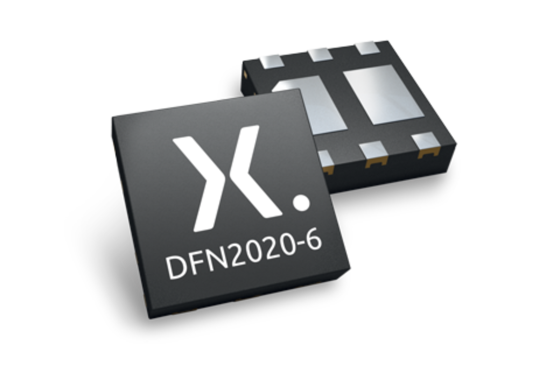
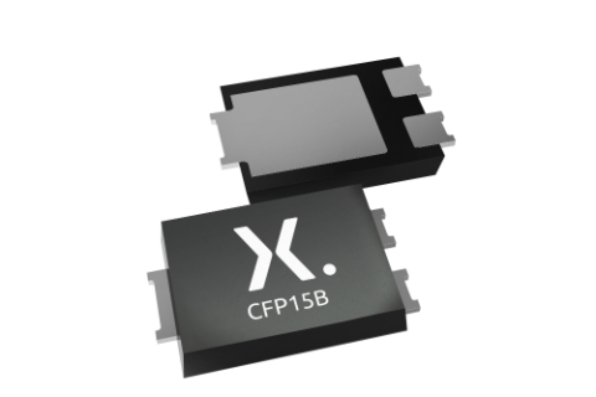
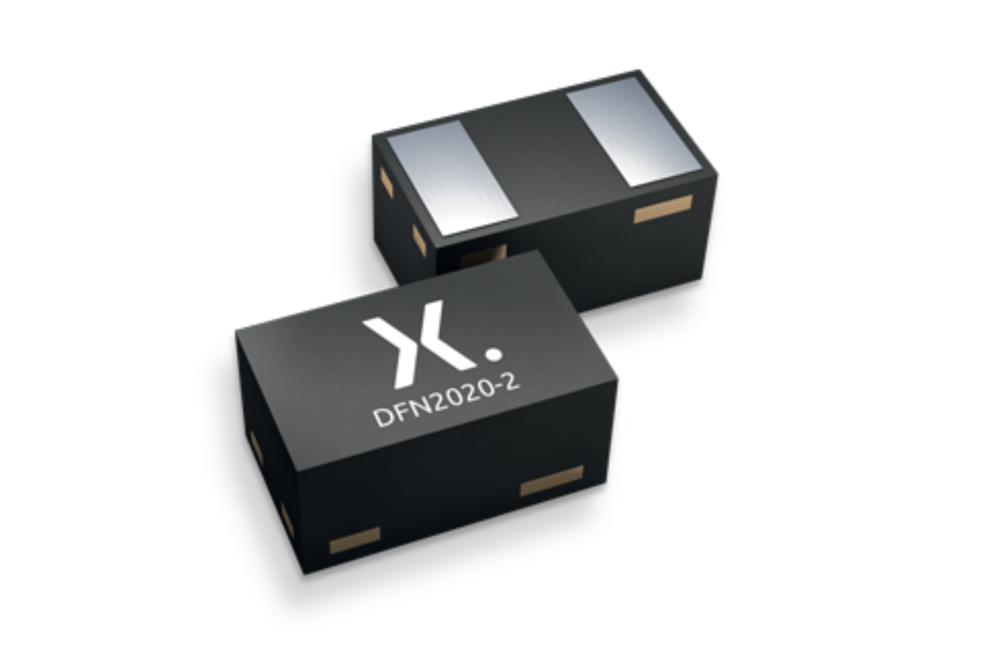
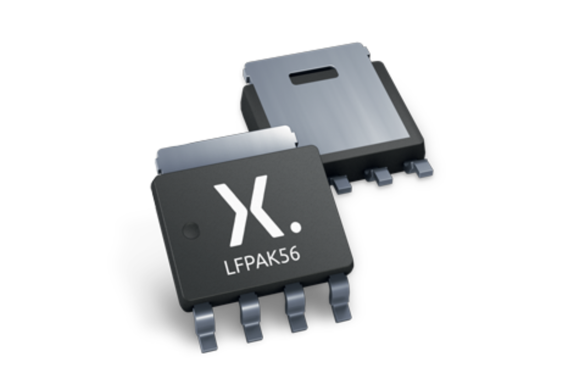
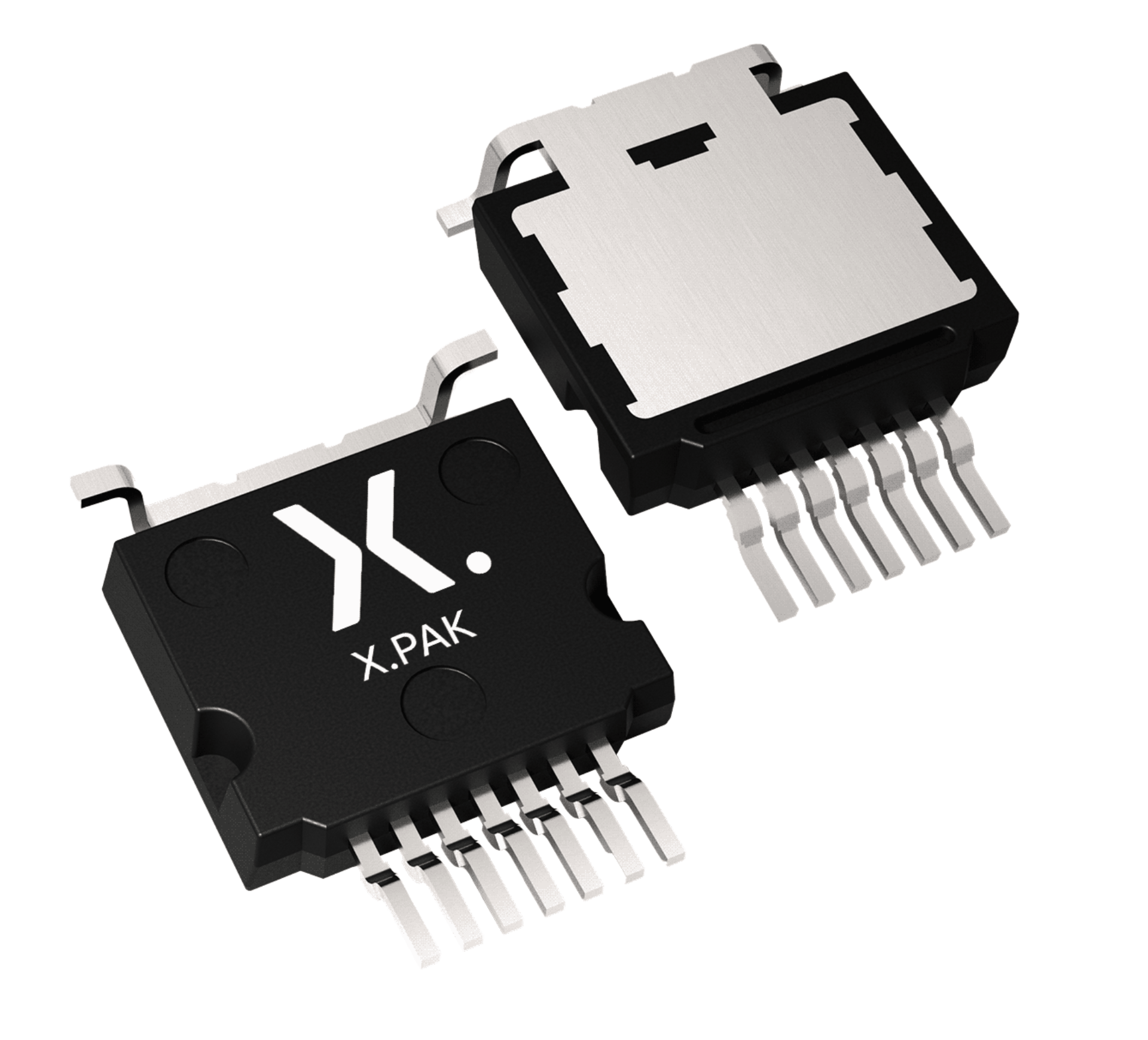
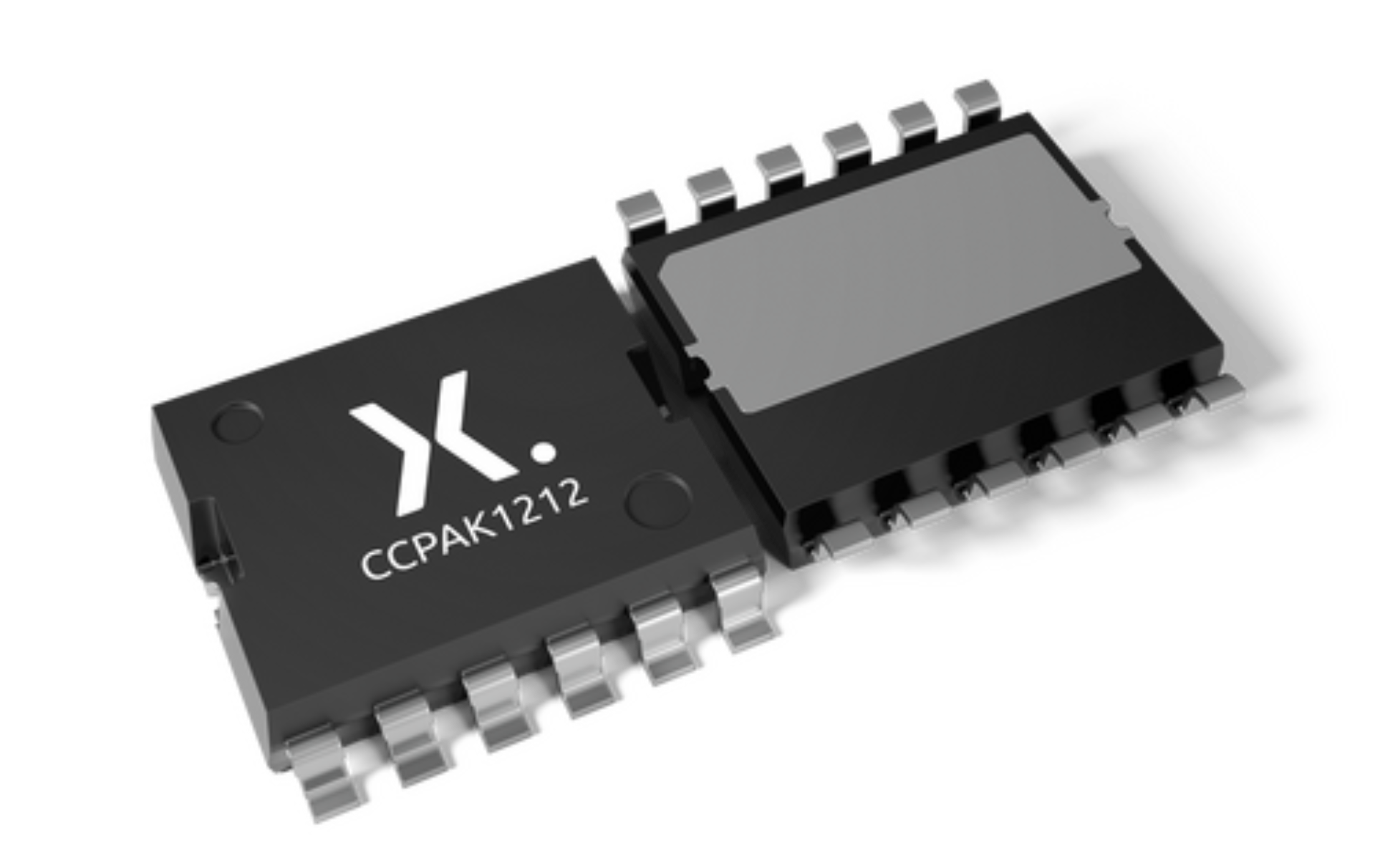
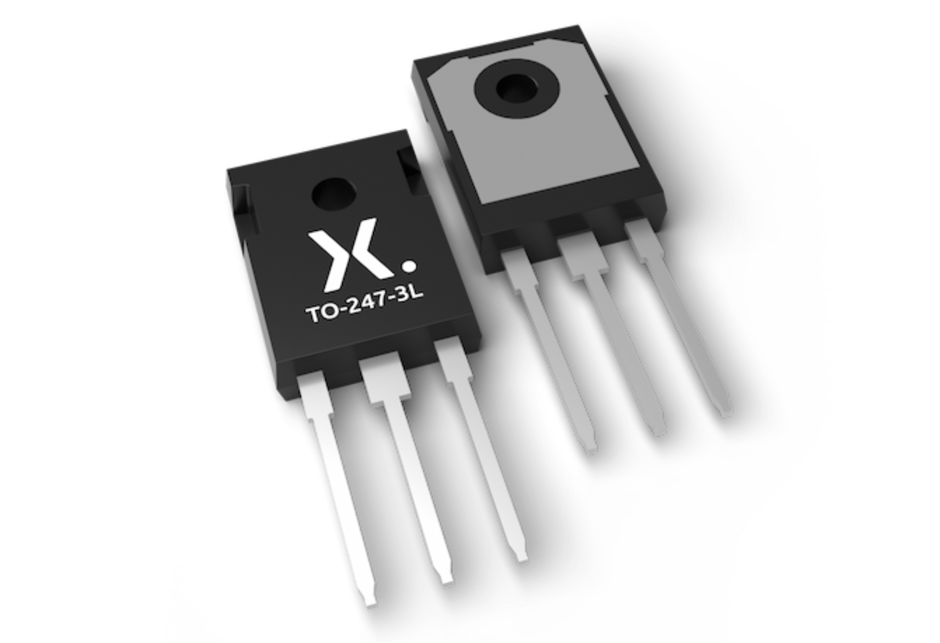
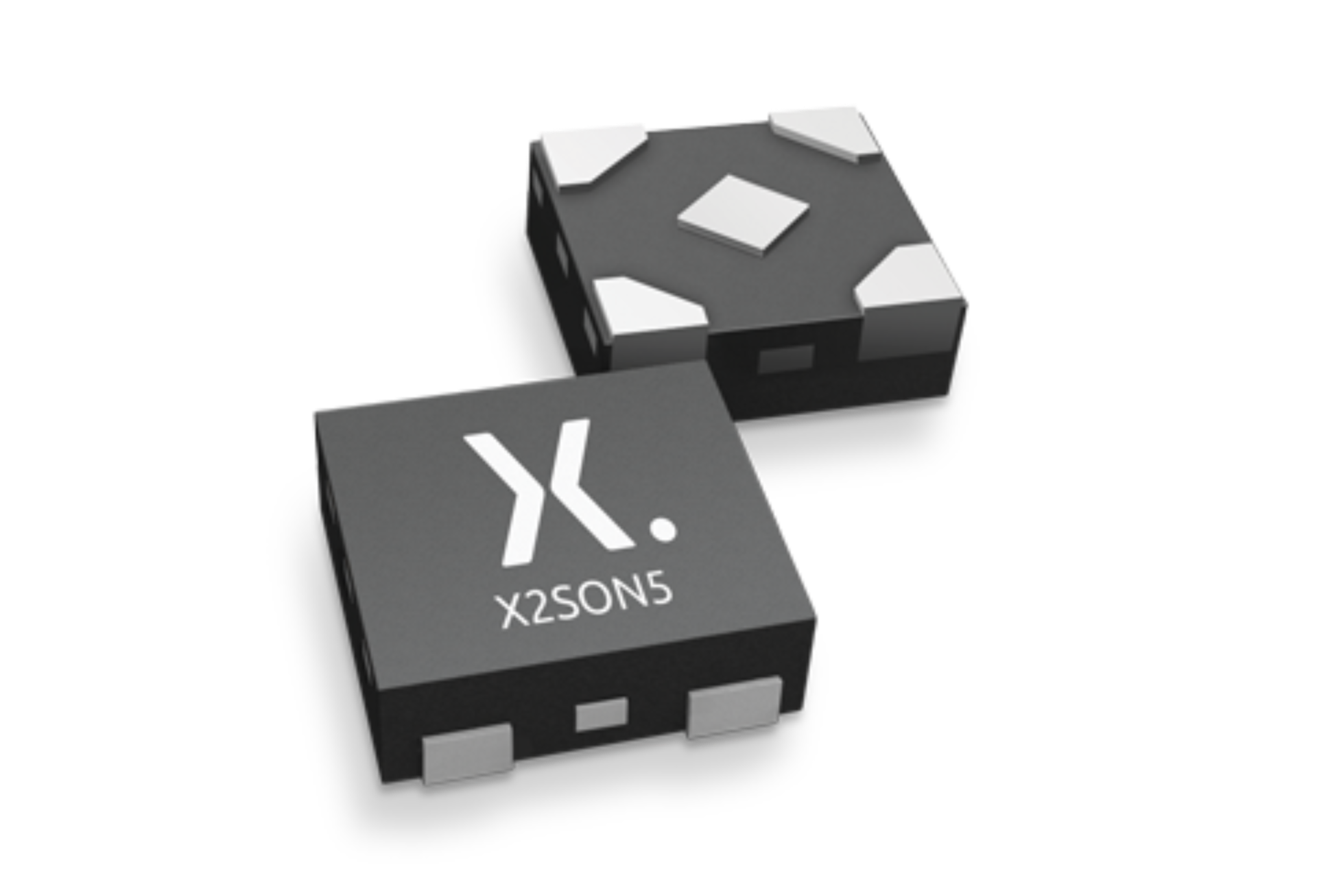
With rapidly evolving requirements, there is a pressing demand for smaller footprints now prevalent throughout most markets for electronic products. Space-saving, thermally efficient, and robust semiconductor packages are needed for transistors and diodes. And while for many product generations, designers have relied on established packages like the SOT23 and SMA families, we see the high performing clip-bond and leadless package outlines such as CFP and DFN clearly winning on value for money.
Join us as we look at the space-saving components that are empowering automotive electrification and the transition to power density packaging that is now underway.
How to choose the right package
A device's internal structure strongly affects the thermal resistance of different semiconductor packages, as do different operating conditions. To ensure circuits' safe and reliable operation and decide for the most appropriate package, designers need to understand thermal parameters and heat dissipation pathways. The blog series “Thermal considerations” guides through different semiconductor package types and the ‘thermal characteristics’ sub-section of the datasheet.

Making semiconductors more resilient with strict testing and new packaging
In this article published on Wevolver, we delve into the fascinating world of semiconductor testing, exploring its evolution, changing operating environments and the need for strict quality control measures. Find out why we believe there are no shortcuts when it comes to robust manufacturing and test processes to ensure product reliability. One example is Nexperia's clip-bonded CFP15B FlatPower package which has passed the stringent Board Level Reliability (BLR) specification at a leading automotive supplier.
