


74AHC74-Q100; 74AHCT74-Q100
Dual D-type flip-flop with set and reset; positive-edge trigger
The 74AHC74-Q100; 74AHCT74-Q100 is a high-speed Si-gate CMOS device and is pin compatible with Low-Power Schottky TTL (LSTTL). It is specified in compliance with JEDEC standard No. 7-A.
The 74AHC74-Q100; 74AHCT74-Q100 is a dual positive-edge triggered, D-type flip-flop with individual data inputs (D), clock inputs (CP), set inputs (SD) and reset inputs (RD). It also has complementary outputs (Q and Q).
The set and reset are asynchronous active LOW inputs that operate independent of the clock input. Information on the data input is transferred to the Q output on the LOW to HIGH transition of the clock pulse. The data inputs must be stable one set-up time prior to the LOW to HIGH clock transition for predictable operation.
Schmitt-trigger action in the clock input makes the circuit highly tolerant to slower clock rise and fall times.
This product has been qualified to the Automotive Electronics Council (AEC) standard Q100 (Grade 1) and is suitable for use in automotive applications.
Features and benefits
Automotive product qualification in accordance with AEC-Q100 (Grade 1)
Specified from -40 °C to +85 °C and from -40 °C to +125 °C
Balanced propagation delays
All inputs have Schmitt-trigger actions
Inputs accept voltages higher than VCC
Input levels:
For 74AHC74-Q100: CMOS level
For 74AHCT74-Q100: TTL level
ESD protection:
HBM: ANSI/ESDA/JEDEC JS-001 class 2 exceeds 2000 V
CDM: ANSI/ESDA/JEDEC JS-002 class C3 exceeds 1000 V
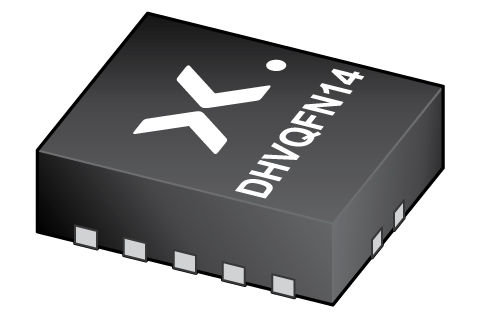
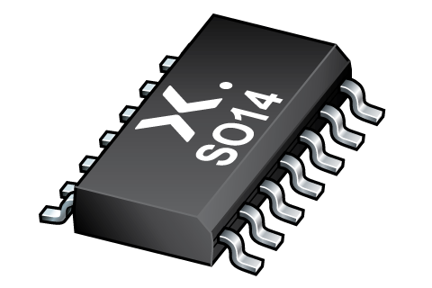
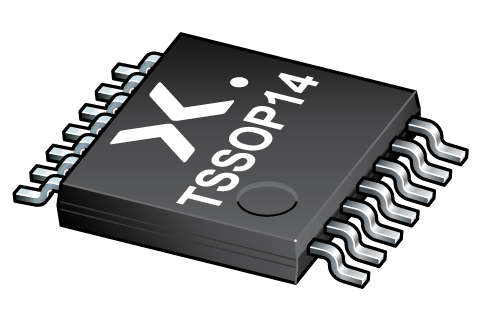
Multiple package options
DHVQFN package with Side-Wettable Flanks enabling Automatic Optical Inspection (AOI) of solder joints
Parametrics
| Type number | VCC (V) | Logic switching levels | Output drive capability (mA) | tpd (ns) | fmax (MHz) | Power dissipation considerations | Tamb (°C) | Rth(j-a) (K/W) | Ψth(j-top) (K/W) | Rth(j-c) (K/W) | Package name |
|---|---|---|---|---|---|---|---|---|---|---|---|
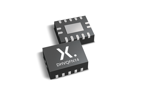
| 74AHC74BQ-Q100 | 2.0 - 5.5 | CMOS | ± 8 | 3.7 | 170 | low | -40~125 | 106 | 20.9 | 74 | DHVQFN14 |
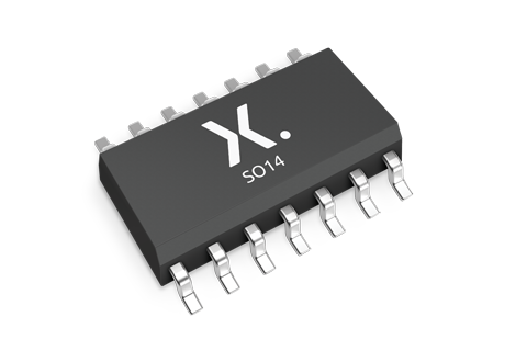
| 74AHC74D-Q100 | 2.0 - 5.5 | CMOS | ± 8 | 3.7 | 170 | low | -40~125 | 108 | 20.1 | 66 | SO14 |
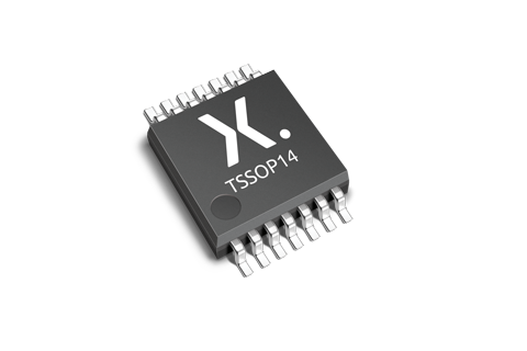
| 74AHC74PW-Q100 | 2.0 - 5.5 | CMOS | ± 8 | 3.7 | 170 | low | -40~125 | 141 | 7.8 | 68 | TSSOP14 |
| 74AHCT74BQ-Q100 | 4.5 - 5.5 | TTL | ± 8 | 3.3 | 160 | low | -40~125 | 106 | 20.9 | 74 | DHVQFN14 |
| 74AHCT74D-Q100 | 4.5 - 5.5 | TTL | ± 8 | 3.3 | 160 | low | -40~125 | 108 | 20.1 | 66 | SO14 |
| 74AHCT74PW-Q100 | 4.5 - 5.5 | TTL | ± 8 | 3.3 | 160 | low | -40~125 | 141 | 7.8 | 68 | TSSOP14 |
Package
| Type number | Orderable part number, (Ordering code (12NC)) | Status | Marking | Package | Package information | Reflow-/Wave soldering | Packing |
|---|---|---|---|---|---|---|---|
| 74AHC74BQ-Q100 | 74AHC74BQ‑Q100X (935300322115) |
Active | AHC74 |
DHVQFN14 (SOT762-1) |
SOT762-1 | SOT762-1_115 | |
| 74AHC74D-Q100 | 74AHC74D‑Q100J (935300323118) |
Active | 74AHC74D |
SO14 (SOT108-1) |
SOT108-1 |
SO-SOJ-REFLOW
SO-SOJ-WAVE WAVE_BG-BD-1 |
SOT108-1_118 |
| 74AHC74PW-Q100 | 74AHC74PW‑Q100J (935300324118) |
Active | AHC74 |
TSSOP14 (SOT402-1) |
SOT402-1 |
SSOP-TSSOP-VSO-WAVE
|
SOT402-1_118 |
| 74AHCT74BQ-Q100 | 74AHCT74BQ‑Q100X (935300325115) |
Active | AHT74 |
DHVQFN14 (SOT762-1) |
SOT762-1 | SOT762-1_115 | |
| 74AHCT74D-Q100 | 74AHCT74D‑Q100J (935300326118) |
Active | 74AHCT74D |
SO14 (SOT108-1) |
SOT108-1 |
SO-SOJ-REFLOW
SO-SOJ-WAVE WAVE_BG-BD-1 |
SOT108-1_118 |
| 74AHCT74PW-Q100 | 74AHCT74PW‑Q100J (935300327118) |
Active | AHCT74 |
TSSOP14 (SOT402-1) |
SOT402-1 |
SSOP-TSSOP-VSO-WAVE
|
SOT402-1_118 |
Environmental information
| Type number | Orderable part number | Chemical content | RoHS | RHF-indicator |
|---|---|---|---|---|
| 74AHC74BQ-Q100 | 74AHC74BQ‑Q100X | 74AHC74BQ-Q100 |
|
|
| 74AHC74D-Q100 | 74AHC74D‑Q100J | 74AHC74D-Q100 |
|
|
| 74AHC74PW-Q100 | 74AHC74PW‑Q100J | 74AHC74PW-Q100 |
|
|
| 74AHCT74BQ-Q100 | 74AHCT74BQ‑Q100X | 74AHCT74BQ-Q100 |
|
|
| 74AHCT74D-Q100 | 74AHCT74D‑Q100J | 74AHCT74D-Q100 |
|
|
| 74AHCT74PW-Q100 | 74AHCT74PW‑Q100J | 74AHCT74PW-Q100 |
|
|
Documentation (18)
| File name | Title | Type | Date |
|---|---|---|---|
| 74AHC_AHCT74_Q100 | Dual D-type flip-flop with set and reset; positive-edge trigger | Data sheet | 2024-03-07 |
| AN90063 | Questions about package outline drawings | Application note | 2025-10-22 |
| SOT762-1 | 3D model for products with SOT762-1 package | Design support | 2019-10-03 |
| SOT108-1 | 3D model for products with SOT108-1 package | Design support | 2020-01-22 |
| SOT402-1 | 3D model for products with SOT402-1 package | Design support | 2023-02-02 |
| ahc74 | ahc74 IBIS model | IBIS model | 2013-04-08 |
| ahct74 | ahct74 IBIS model | IBIS model | 2013-04-08 |
| Nexperia_package_poster | Nexperia package poster | Leaflet | 2020-05-15 |
| DHVQFN14_SOT762-1_mk | plastic, dual in-line compatible thermal enhanced very thin quad flat package; no leads; 14 terminals; 0.5 mm pitch; 2.5 mm x 3 mm x 0.85 mm body | Marcom graphics | 2017-01-28 |
| SO14_SOT108-1_mk | plastic, small outline package; 14 leads; 1.27 mm pitch; 8.65 mm x 3.9 mm x 1.75 mm body | Marcom graphics | 2017-01-28 |
| TSSOP14_SOT402-1_mk | plastic, thin shrink small outline package; 14 leads; 0.65 mm pitch; 5 mm x 4.4 mm x 1.1 mm body | Marcom graphics | 2017-01-28 |
| SOT762-1 | plastic, leadless dual in-line compatible thermal enhanced very thin quad flat package; 14 terminals; 0.5 mm pitch; 2.5 x 3 x 1 mm body | Package information | 2023-04-05 |
| SOT108-1 | plastic, small outline package; 14 leads; 1.27 mm pitch; 8.65 mm x 3.9 mm x 1.75 mm body | Package information | 2023-11-07 |
| SOT402-1 | plastic, thin shrink small outline package; 14 leads; 0.65 mm pitch; 5 mm x 4.4 mm x 1.2 mm body | Package information | 2023-11-07 |
| SO-SOJ-REFLOW | Footprint for reflow soldering | Reflow soldering | 2009-10-08 |
| SO-SOJ-WAVE | Footprint for wave soldering | Wave soldering | 2009-10-08 |
| WAVE_BG-BD-1 | Wave soldering profile | Wave soldering | 2021-09-08 |
| SSOP-TSSOP-VSO-WAVE | Footprint for wave soldering | Wave soldering | 2009-10-08 |
Support
If you are in need of design/technical support, let us know and fill in the answer form we'll get back to you shortly.
Models
| File name | Title | Type | Date |
|---|---|---|---|
| SOT762-1 | 3D model for products with SOT762-1 package | Design support | 2019-10-03 |
| SOT108-1 | 3D model for products with SOT108-1 package | Design support | 2020-01-22 |
| SOT402-1 | 3D model for products with SOT402-1 package | Design support | 2023-02-02 |
| ahc74 | ahc74 IBIS model | IBIS model | 2013-04-08 |
| ahct74 | ahct74 IBIS model | IBIS model | 2013-04-08 |
Ordering, pricing & availability
Sample
As a Nexperia customer you can order samples via our sales organization.
If you do not have a direct account with Nexperia our network of global and regional distributors is available and equipped to support you with Nexperia samples. Check out the list of official distributors.