


Authors: Christian Radici and Andrew Thomson, Applications engineers, Manchester
This interactive application note contains embedded Cloud based simulations to augment the text.
To open the embedded simulation, simply hover over the simulation image. Left click anywhere in the graphic area once the central play button changes in colour. This opens the schematic in the Cloud environment. See the interactive application note tutorial page for more details on how to use the simulations.
See accompanying application note: AN50007.
1. Introduction
In terms of model accuracy, ease of use and data generation, today’s electrical simulation tools are a world away from their early command line driven ancestors. During the Automotive product development process key stage testing is performed at Design and Process Validation phases. Test failures during these phases have serious consequences on remedial costs and program timing. Simulation can be used to good effect to expose design weaknesses and improve product robustness to EMC at an early stage during product development. Diligent bench work to verify the design improvements indicated by simulation will therefore reduce the likelihood of such late occurring EMC compliance failures.
This interactive application note examines the effect of applying a selection of conducted battery line transients to Reverse Battery Protection (RBP) circuits. Simulations of RBP circuits using an N-Channel MOSFET, BUK7Y7R8-80E are included. The battery line transients are described in ISO 21780:2020 for 48 V systems and in ISO 7637-2:2011, ISO 16750-2:2012 §4.6.4 for 12 V/24 V battery systems. These specifications apply to road vehicles.
Losses in RBP applications are predominantly due to conduction losses. i.e. current flow through the MOSFET channel on resistance, RDSon. To reduce dissipation in 12 V and 24 V systems the engineer has a choice to use a lower Drain to Source Voltage (VDS) rated part to achieve a lower RDSon e.g. BUK7Y4R8-60E. Dissipation is given by the product of the square of the Drain current and channel resistance, ID2 * RDSon so changing from a 7.8 mΩ part to a 4.8 mΩ lowers dissipation by 4.8/7.8*100% or ~60%.
The intention here is to illustrate what is happening to the MOSFET (the immunity it has to the ISO pulse) in-circuit so that its safe operating parameters are respected. Examples are used for the illustrations with detailed narrative to explain the context of the test within the vehicle environment. Although the ISO specifications are largely prescriptive in some cases OEMs do have liberty to apply them in terms of specifying certain boundary conditions e.g. source generator voltage or resistance.
References are made to an interactive Cloud based simulation tool where baseline circuits have been constructed and the reader is encouraged to experiment with the simulations within those boundary conditions. All circuitry is predicated upon N-Channel MOSFET devices operating in an ambient temperature of 23 ±5 °C per guideline.
Five conducted immunity transients are discussed.
- ISO 7637-2:2011 pulse 1 for 12 V systems having to be immune to supply line disconnections which produce large negative transients
- ISO 7637-2:2011 pulse 1 for 24 V systems having to be immune to supply line disconnections which produce large negative transients
- ISO 16750-2:2012 §4.6.4 for 12 V & 24 V systems with Test A applied for systems having to be immune to Unsuppressed Load Dump transients
- ISO 16750-2:2012 §4.6.4 for 12 V & 24 V systems with Test B applied for those systems with Centralized Load Dump protection
- ISO 21780:2020 Test-03: Short term overvoltage and Test-04: supply component load dump control test.
The iso.org website indicates at some future date replacement of the above by ISO/CD 7637-2 and ISO 16750-2 by ISO/AWI 16750.
2. Transient pulse descriptions for 12 V and 24 V battery systems

2.1. ISO 7637-2 pulse 1
The specification makes mention of methods to monitor fast and slow emission transients but the focus here is on modelling the immunity test set up of the DUT.
The waveshape is designed to mimic a situation where the battery supply is disconnected.
Referring to Fig. 1, after disconnection from the source by S1 the Device Under Test (DUT) is exposed to the negative going voltages or back EMF transients produced by the collapse of magnetic fields in neighbour inductive loads on the same supply line as the DUT.
Examples of disconnection given in the specification are of a fuse being blown or pulled, there may be a disconnection/break in the harness supply or simply an open circuit as a result of turning off the ignition switch.
Although in some systems the ignition line is simply a low current signal into a DUT which contains circuitry to switch on an external Main Power Relay or internal Solid State Relay, in this application note we consider the connections as described below.
Fig. 1 helps visualise how the DUT can be affected by the inductive loads in the system. Once S1 ignition switch opens the back EMF transient produced is conducted into the DUT. The load resistance in parallel with the DUT is that created by the other devices sharing the same power NET. The harness forms loop resistances with these neighbour devices. The Original Equipment Manufacturer has visibility of the system and can define the value of this parallel load resistance Rs in the Customer Requirement Document.
2.2. Simulating the conducted immunity transient - test waveform
Fig. 1 indicates when such a conducted transient will develop. The wave shape shown in Fig. 2 and parameter settings given in Table 1 reveal the configuration of the ISO 7637-2 pulse 1 model used in the simulation. Note the specification allows for tolerance whereas the simulation models use the fixed values shown.

|
Parameter |
Nominal 12 V system |
12 V pulse model |
Nominal 24 V system |
24 V pulse model |
|
UA |
13.5 V ±0.5 V |
13.5 V |
27 V ±1 V |
27 V |
|
Us |
−75 V to −150 V |
−75 V |
−300 V to −600 V |
−300 V |
|
Ri |
10 Ω |
10 Ω |
50 Ω |
50 Ω |
|
td |
2 ms |
2 ms |
1 ms |
1 ms |
|
tr |
1 +0/-0.5 μs |
1 μs |
3 μs |
3 μs |
|
t1 |
≥ 0.5 s |
0.5 s |
≥ 0.5 s |
0.5 s |
|
t2 |
200 ms | |||
|
t3 |
<100 μs |
100 μs |
<100 μs |
100 μs |
| t1 shall be chosen such that it is the minimum time for the DUT to be correctly initialized before the application of the next pulse and shall be ≥ 0.5 s | ||||
| t3 is the smallest possible time necessary between the disconnection of the supply source and the application of the pulse. | ||||
2.3. Simulating the conducted immunity transient - test setup
ISO 7637-2 goes into great detail of how to achieve the correct setup with the real world product, particularly how to verify the open load test waveform from the test generator. In simulation the situation is made easier in that the ISO transient source is configured to output the starting value of the battery voltage UA and then faithfully reproduces the remainder of the waveform.
2.3.1. Artificial network
Using an artificial network as in Fig. 3 removes real life variation in the measurement result which would otherwise occur from differences in vehicle wiring harness impedances. The network therefore provides a standard reference laboratory environment for equipment to determine the behaviour of electrical and electronic devices. In other words it is possible to test products at different accredited test houses and expect reliably comparable results from each.

- Inductor L = 5 µH
- Internal resistance between terminals P and A < 5 mΩ
- Capacitor C = 0.1 µF for working voltages of 200 VAC 1,500 VDC
- Resistor R = 50 Ω

ISO 7637-2 indicates the frequency response of the network, where terminal A and B are shorted together and the impedance is obtained looking into P with respect to B, see Fig. 4.
In simulation we can model the above response quite easily but having so many different real world circuit configurations it is not possible to faithfully model all of them. In lieu the baseline simulation offers an insight as to what happens to the MOSFET when the pulse appears inside the product.
Click the arrow to run simulation 1: ISO 7637-2 Pulse 1 - 12 V
Simulation 1. ISO 7637-2 Pulse 1 - 12 V
The simulation comprises ISO pulse generator, DUT with its corresponding thermal model and an additional circuit used to verify the avalanche capability against data sheet specs.
The ISO generator outputs 500 pulses every 0.5 s. Its series resistance is set depending on the system battery voltage, it is 10 Ω in case of a 12 V system and 50 Ω for a 24 V one.
The DUT is a series NMOS used to protect the load from reverse polarity conditions, feeding a parallel RC load. An ideal voltage generator is used to model a charge pump that would be needed in the actual application to correctly bias the gate of the MOSFET, ideally 10 V above the battery rail voltage. Additionally a BJT has been used to turn OFF the MOSFET (by shorting its gate to ground) when the reverse polarity condition is met.
The thermal model is used to monitor the variation in temperature of the junction. The Electrical Power to Heat Flow block is used to convert the electrical power calculated as VDS × ID into heat flow that the thermal circuit will be able to handle. This block is also useful to directly monitor the drain current and drain to source voltage of the MOSFET, simply by probing for I_sense and V_sense, respectively. Notice how the ambient temperature is being set at 25 °C by using the Thermal Ambient Reference block at the bottom of the RC network. An additional RC network has been added to the NMOS Cauer model in order to take into account the PCB thermal behaviour (FR4).
Finally an additional circuit is used to verify that the MOSFET is operating within specification during avalanche. The avalanche test circuit is composed of an inductor of 7 mH with a series resistance of 5 Ω. These two components are chosen in order to replicate the conditions at which the MOSFET is subjected to when used in the ISO pulse circuit, during the avalanche event. The inductor is in fact charged at the same peak current of 6.7 A and the drain voltage is set at 66.2 V. Only afterwards, the switch is opened and the energy stored in the inductor is discharged through the MOSFET. The shape of the current and duration of the event remain almost the same. An external thermal network is employed to verify that the junction temperature in the two cases reaches the same temperature, about 46 °C for a power peak of ~460 W.
Click the arrow to run simulation 2: ISO 7637-2 Pulse 1 - 24 V
Simulation 2. ISO 7637-2 Pulse 1 - 24 V

The BUK7Y4R8-60E is seen connected in series with the bulk electrolytic capacitance and internal loads. As the negative transient appears on the supply line the MOSFET remains enhanced for a time. This means the Gate pin with respect to its Source pin (VGS) remains positive and greater than its threshold voltage VGS(th).
During enhancement the MOSFET places a Drain to Source channel resistance (RDSon) in parallel with its Source to Drain DIODE. Additionally the MOSFET allows Drain current to flow in either direction through the channel resistance.
Energy stored in the bulk electrolytic capacitance can be drained by the negative-going pulse from the generator. Nexperia defines VGS(th) when 1 mA Drain current flows in the channel. VGS(th) has a negative temperature coefficient. Since Electromagnetic Compliance Testing (EMC) is conducted in an ambient close to 25 °C we should expect the threshold to be somewhere below 4 V as indicated in the table below. Hence as the battery supply becomes more negative at some point the charge pump will turn off and VGS will fall below its VGS(th). The MOSFET enters its sub-threshold region (turns OFF).
Nexperia guarantees the MOSFET to be in its Sub-threshold region (DIODE mode) if VGS ≤ 1 V for any temperature. The simulation uses a BJT to switch off the gate bias when VGS ≤ 1 V.
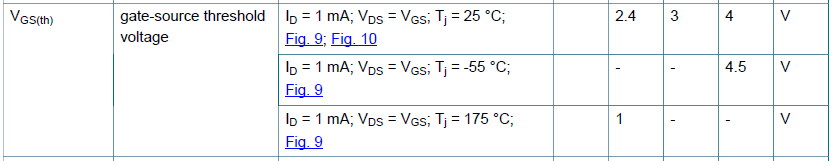
Figure 6. BUK7Y4R8-60E gate-source threshold charactertistics

As the pulse continues in its negative direction the MOSFET, now behaving as a blocking DIODE, will begin to leak appreciably when the negative bias across it reaches a voltage 10% greater than the MOSFETs rated VDS and by 30% will be in full avalanche.
The test requires 500 pulses to be applied. Each time the voltage across the device exceeds -1.3 × VDS rating the MOSFET will be in avalanche. We have a choice either to ensure the component can withstand the repetitive avalanche energy or prevent avalanche by fitting a TVS suppressor across the product’s battery supply.
Note an optional bidirectional TVS is shown. Dependent on budget and PCB real estate availabe this may be two anti-series unidirectional types or one bidirectional as shown.

Note from the above statement we have an expression for the avalanche breakdown voltage:
VBR ≈ 1.3 × V(BR)DSS
The negative sign in the description above (not present in the above expression) is only to indicate that a negative bias is being applied to the anode with respect to the cathode to cause avalanche. Normally we consider the reverse bias case as a positive bias being applied to the cathode with respect to the anode as shown in the graph of Fig. 8.
- V(BR)DSS is the breakdown voltage voltage when 250 µA leaks through the reverse biased diode
- V(BR)DSS is stated in the data sheet for a particular device
- VDD shown in the Fig. 8 is the equivalent of system votage UA
The simulation shows the voltage, current and power dissipated by the MOSFET diode during the negative transient event when connected as an RBP pass element as above. What is needed is some way to reliably replicate the exposure of the MOSFET to the energy normally seen in an avalanche event and decide whether the 500 ISO pulses can be considered as repetitive or single events. Hence there are two circuits in the simulation one for the RBP above and the other for an avalanche (AKA Unclamped Inductive Switching or UIS) event.
The diagrams below show the anatomy of the UIS waveform. Note the controlled linear current ramp produced by having an inductive load which helps to accurately describe the energy dissipated by the MOSFET during the event.
|

Figure 9: Gate-source voltage VGS |

Figure 10: Drain-source voltage VDS |

Figure 11: Drain current, ID |
|

Figure 12: Peak drain-source avalanche power, PDS(AL)M |

Figure 13: Transient junction temperature profile of MOSFET during an avalanche event |
|

Fig. 14 below shows how the single event above translates to repetitive UIS. As long as the energy absorbed by the MOSFET remains within safe operting limits for one event the MOSFET is expected to survive > 100 x 10^6 avalanche events, refer to Fig. 15. Having only 500 ISO pulses applied, the task here is to ensure the device can survive that first ISO pulse.

Figure 14. Drain-source voltage, VDS and repetitive drain-source avalanche current, IDS(AL)R
The current profile of the 12 V UIS simulation has been modified with a 7 mH inductance such that the current peak, rise and fall times closely match that of the current profile of the 12 V RBP MOSFET. The combinational graph shown in Fig. 16 (MOSFET waveforms) is taken from simulation for the RBP MOSFET and Fig. 17 (Avalanche current) is taken from the avalanche analogy.
|
Figure 16. ISO 7637-2 - 12 V Pulse 1 - MOSFET Q1 waveforms |
Figure 17. ISO 7637-2 - 12 V Pulse 1 - MOSFET Q1 and Q2 avalanche current waveforms |


Fig. 18 below shows the check of junction temperature rise from 12 V RBP simulation (green trace) versus that of the UA = 12 V avalanche simulation.
|
Figure 18. ISO 7637-2 - 12 V Pulse 1 - MOSFET Q1 and Q2 junction temperature waveforms |


Curve (1) of Fig. 19 is the reference curve for safe operation of the BUK7Y4R8-60E for a single event with a junction temperature Tj starting from 25 °C.
Referring to Fig. 12, the peak drain-source avalanche power (PDS(AL)M) dissipated in the MOSFET was shown to be the product of the breakdown voltage (VBR) and the non-repetitive drain-source avalanche current (IDS(AL)S).
(Eq. 1) 
The avalanche simulation gives values for breakdown voltage, avalanche time and peak breakdown current:
- VBR = 1.3 * 60 = 78 V
- tAL = 86.5016 - 86.5011 = 500 μs
- Ipk = 6.7111498 A
Substituting these values in Equation 1 we obtain:
EDS(AL)S = (78 V * 6.7111498A * 500 µs) /2 = 130.87 mJ, which can be safely absorbed by the MOSFET.
Adding coordinate lines for IAL = 6.7 A and tAL = 500 μs to the adjacent graph (Fig. 19) confirms we are well inside the safe operating area inscribed by curve (1).

Figure 20. BUK7Y4R8-60E data sheet extract: EDS(ALS) and V(BR)DSS

3. ISO 16750-2 section 4.6.4 load dump
Consider what would happen if for instance a vehicle were undergoing maintenance while the engine was running. The alternator is charging the battery and providing power for the vehicle and in good regulation holding the battery supply lines somewhere between 13.5 V to 14.5 V, typically 14.2 V for a nominal 12 V system.
An alternator’s output is controlled by the current flow in the field winding. The larger the field current the greater the output current from the alternator. Stator and field windings have large inductances so changes in field current to provide regulation follow a trend rather than a step.
Assume the battery is in a poor state of charge and providing a heavy load when it is disconnected from the system. This loss of load (load dump) is a step change which happens much faster than the regulator’s ability to reduce the current in the field winding. The energy available from the alternator at this time is much greater than the system requires.
The energy required from the alternator is the system power consumption for the time of the demand, given by:
Energy = Power × time = Voltage × Current × time (measured in the derived Watt-second unit) where 1 Ws = 1 Joule.
When the battery is disconnected, load current will drop by an amount, for the sake of simplicity let’s imagine this amount to be half the present system current. Due to regulation latency at the moment of disconnection the equality for our example becomes:
(Eq. 2) 
i.e. the decrease in load current is being compensated for by an increase in output voltage from the alternator and will persist until the field current is reduced by the regulator.
In our simplified example above the implication is that the peak voltage appears as a step change whereas in reality the rise in voltage is not instantaneous but rather limited by circuit dynamics. The behaviour is better described by the waveshapes of the ISO16750-2 pulses which are based on estimation from real life experience.
Some of the ISO transient pulses can be destructive. Load dump pulses are particularly good candidates to expose design weaknesses. An under-rated TVS will usually fail short circuit or very low resistance but semiconductors have the potential to fail with some level of impairment other than a short circuit. A full short circuit or very low resistance failure can be viewed as beneficial when performing DFMEA assessment as the failure is highly detectable at system level. An open circuit or impaired TVS is much more difficult to assess.
3.1. Simulating test waveform ISO 16750-2 section 4.6.4 - test A
Systems which do not have a means of controlling output voltage from the alternator have to be able to cope with unsuppressed load dump pulses. The amplitude of the test waveform is significantly higher than the suppressed alternator voltage described in Test Pulse B.

Key for Fig. 22:
| U | test voltage | |
| td | duration of pulse | |
| tr | rising slope | |
| UA | supply voltage for generator in operation | |
| US | supply voltage |
|
Parameter |
Type of system |
Minimum test requirements | |
|
UN = 12 V |
UN = 24 V |
||
|
Us [a] (V) |
79 ≤ US ≤ 101 |
151 ≤ US ≤ 202 |
10 pulses at 1 min intervals
|
|
Ri [a] (Ω) |
0.5 ≤ Ri ≤ 4 |
1 ≤ Ri ≤ 8 |
|
|
td (ms) |
40 ≤ td ≤ 400 |
100 ≤ td ≤ 350 |
|
|
tr (ms) |
10 |
10 |
|
|
[a] If not otherwise agreed; use the upper voltage level with the upper value for the internal resistance, or use the lower voltage with the lower value for the internal resistance. |
|||
The internal resistance, Ri, of the load dump test pulse generator can be obtained as follows:
(3) 
where:
- Unom is the specified voltage of the alternator
- Irated is the specified current at an alternator speed of 6,000 min-1
- Nact is the actual alternator speed, in reciprocal minutes
The simulations comprise the ISO pulse generator and DUT with the corresponding thermal model.
The ISO generator outputs 10 pulses with an interval of 60 s after the voltage returns to its nominal system voltage value. Its series resistance is set depending on the system battery voltage, it is 0.5 Ω in case of a 12 V system and 1 Ω for a 24 V one. Notice that the generator has been equipped with a series resistance of 0.5 Ω for the 12 V system and 1 Ω for the 24 V system.
The DUT is a series NMOS used to protect the load from reverse polarity conditions feeding a parallel RC load. An ideal voltage generator is used to model a charge pump that would be needed in the actual application to correctly bias the gate of the FET ideally 10 V above the battery rail voltage.
The thermal model is used to indicate the variation in temperature of the junction. The Electrical Power to Heat Flow block converts electrical power calculated as VDS·ID into heat flow that the thermal circuit will be able to handle. This block is also useful to directly monitor the drain current and drain to source voltage of the FET, simply by probing for I_sense and V_sense, respectively. Notice how the ambient temperature is being set at 25 °C by using the Thermal Ambient Reference block at the bottom of the RC network. An additional RC network has been added to the NMOS Cauer model in order to take into account the PCB thermal behaviour (FR4).
In the 12 V simulation dissipating a peak power of ~ 3.5 W, the FET junction temperature is expected to rise to 25.35 °C.
In the 24 V simulation dissipating a peak power of ~ 3.5 W, the FET junction temperature is expected to rise to 25.7 °C.
Click the arrow to run simulation 3: ISO16750-2 - 12 V Test A
Simulation 3. ISO16750-2 - 12 V Test A
Click the arrow to run simulation 4: ISO16750-2 - 24 V Test A
Simulation 4. ISO16750-2 - 12 V Test A
4. Simulating test waveform ISO 16750-2 for section 4.6.4 - test B
The waveshape shown in Fig. 23 is for 12 V and 24 V systems which have Central Load Dump Protection. This means that some form of extremely capable transient suppression is present within the alternator to hold its output below a certain voltage. This is achieved by replacing the Recovery Rectifiers of the three phase bridge with Zener Diodes.

The voltage waveform is very similar to that of the pulse for Test A except the peak of the waveform has been clipped due to the Zener function in the alternator’s output rectifier bridge.
If further suppression is needed to protect components inside the product then a suitably sized Transient Voltage Suppressor (TVS) can be selected.
TVS devices function as very fast Zener diodes. The lower the breakdown voltage (VBR) chosen for the TVS, the earlier in the transient waveform it will begin to conduct and the higher the dissipation throughout the remainder of the pulse.

Key for Fig. 23:
| U | test voltage | |
| td | duration of pulse | |
| tr | rising slope | |
| UA | supply voltage for generator in operation | |
| US | supply voltage | |
| *US | supply voltage with load dump suppression |
|
Parameter |
Type of system |
Minimum test requirements | |
|
UN = 12 V |
UN = 24 V |
||
|
Us [a] (V) |
79 ≤ US ≤ 101 |
151 ≤ US ≤ 202 |
5 pulses at 1 min intervals
|
|
Us [a] (V) |
79 ≤ US ≤ 101 |
As specified by customer (typical value 58 V) | |
|
Ri [a] (Ω) |
0.5 ≤ Ri ≤ 4 |
1 ≤ Ri ≤ 8 |
|
|
td (ms) |
40 ≤ td ≤ 400 |
100 ≤ td ≤ 350 |
|
|
t3 (ms) |
10 |
10 |
|
|
[a] If not otherwise agreed; use the upper voltage level with the upper value for the internal resistance, or use the lower voltage with the lower value for the internal resistance. |
|||
The simulations comprise the ISO pulse generator and DUT with the corresponding thermal model. The ISO generator outputs 5 pulses with an interval of 60 s after the voltage returns to its nominal system voltage value. Its series resistance is set depending on the system battery voltage, it is 0.5 Ω in case of a 12 V system and 1 Ω for a 24 V one.
The DUT is a series NMOS used to protect the load from reverse polarity conditions feeding a parallel RC load. An ideal voltage generator is used to model a charge pump that would be needed in the actual application to correctly bias the gate of the FET ideally 10 V above the battery rail voltage. The thermal model is used to indicate the variation in temperature of the junction. The Electrical Power to Heat Flow block converts electrical power calculated as VDS·ID into heat flow that the thermal circuit will be able to handle. This block is also useful to directly monitor the drain current and drain to source voltage of the FET, simply by probing for I_sense and V_sense, respectively.
Notice how the ambient temperature is being set at 25 °C by using the Thermal Ambient Reference block at the bottom of the RC network. An additional RC network has been added to the NMOS Cauer model in order to take into account the PCB thermal behaviour (FR4).
Click the arrow to run simulation 5: ISO16750-2 - 12 V Test B
Simulation 5. ISO16750-2 - 12 V Test B
In the 12 V simulation dissipating a peak power of ~ 3.5 W, the FET junction temperature is expected to rise to 27.90 °C.
Click the arrow to run simulation 6: ISO16750-2 - 24 V Test B
Simulation 6. ISO16750-2 - 24 V Test B
In the 24 V simulation dissipating a peak power of ~ 3.5 W, the FET junction temperature is expected to rise to 32.75 °C.
5. Vehicle Electrification Definitions
There are four mainstream categories of vehicles undergoing some form of electrification: Battery Electric Vehicle (BEV); Hybrid Electric Vehicle (HEV); Plug-in Hybrid Electric Vehicle (PHEV) and Mild Hybrid. The capability of electric motors to propel the vehicle independently of the Internal Combustion Engine (ICE) differs with the hybrid vehicle type. Nomenclature for battery chargers may vary from country to country but in general classifications are: Level 1 (L1), Level 2 (L2) and DC Fast Charger (DCFC), each in increasing power capability respectively. L1 and L2 are normally to be found at residential properties. In the UK the residential chargers would be classified as Type 1 (slow typically < 3 kW fully charged in 8-10 hours) or Type 2 (fast typically 7 kW or 22 kW fully charged in 2-4 hours). As vehicle charging technologies improve and high power charging stations of typically 43 kW become more widely availability then charging times will reduce to 30-60 minutes which is no more an imposition than stopping for a break at a motorway service facility.
-
Battery Electric Vehicles (BEVs)
The sole source of energy is provided by battery systems and dependent on vehicle efficiencies. Propulsion for passenger vehicles is provided by three phase induction motors fed from a high voltage (HV) battery system, commonly in the range 360 V to 450 V, - although higher voltage systems are available. The motors are AC machines. Inverters are required to convert from battery DC to construct the AC waveform. In automotive applications the motor has to be able to rotate at varying speeds and torque. The PWM control features available from the inverter make such variable speed control possible.
A 12 V battery is used to provide low tension auxiliary power e.g. for low 5V/12V power outlets, multimedia & lighting.
1 kWh taken from the mains supply will provide approximately 4 miles of range with these HV motors. Balancing the range of electric vehicles between charges with performance has always been the issue. Improvements in battery technologies and charge station availability away from the residential setting are addressing these key factors. e.g. at the time of writing dependent on maker, model and driving style, fast-charge electric vehicle ranges vary from 110 to 373 miles.
-
Hybrid Electric Vehicles (HEVs)
HEVs have ICE and electric motive power. Electrical propulsion for passenger vehicles is provided by three phase induction motors fed from a high voltage (HV) battery system commonly in the range 360 V to 450 V. Higher voltage systems can be found. HEVs can recharge their battery through generators driven from the ICE including overrun and recuperative (regenerative) braking. Dependent on load an HEV can travel for short distances of 1 to 2 miles before resorting to the ICE to provide propulsion and recharge the depleted battery. Dependent on the battery charge state, electric motors can propel the HEV from a standing start. The acceleration is smooth reaching speeds of 30 m.p.h. with seemingly little effort. If a more prolonged acceleration is required the ICE is switched into the powertrain to provide propulsion and recharging of the battery. The ICE is employed at cruising speeds when it can operate most efficiently. A 12 V battery is present to provide low tension auxiliary power e.g. low 5 V/12 V power outlets, multimedia and lighting.
-
Plug-in Hybrid Electric Vehicles (PHEVs)
PHEVs behave similarly to HEVs having both ICE and motors which are capable of providing electric motive power in isolation to the ICE. Electrical propulsion for passenger vehicles is provided by three phase induction motors fed from a high voltage (HV) battery system commonly in the range 360V to 450 V, although higher voltage systems can be found. PHEVs can recharge their battery through generators driven by the ICE including overrun and recuperative (regenerative) braking. PHEVs have a greater battery capacity than HEVs and as the name states the PHEV’s battery is plug-in mains rechargeable. The increased battery capacity permits the PHEV to travel for longer periods on electric power before resorting to the ICE with ranges of 10 to 40 miles being common. A 12 V battery is present to provide low tension auxiliary power e.g. low 5 V/12 V power outlets, multimedia and lighting.
-
Mild hybrid (48 V systems)
In mild hybrid solutions where a conventional 12 V battery system with ICE is supported by a Starter/Generator and DC/DC converter interfaces to the 48 V battery. Electric motors are used to assist the ICE during acceleration and cruising but the motor is unable to power the vehicle in isolation.

6. 48 V Powertrain development
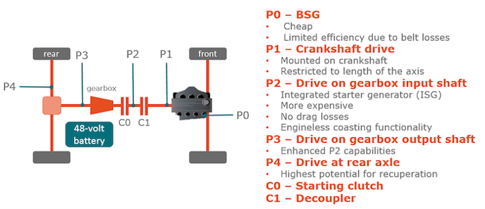
To improve efficiencies further and continue to reduce the vehicle’s C02 footprint alternatives to the 48V on-engine 5kW, 85% efficient BSG are required:
- Mounting Position. Moving the starter generator to another position in the powertrain improves capability and efficiency
- Budget Power and Efficiencies.
Systems are improving all the time, figures given indicate the benefit expected from mounting electrical machines in positions P1-P4 over that of the BSG in P0.
- P1 on-engine, higher torque, no belt losses, 10kW, 94% efficient
- P2 gearbox input shaft either integral or side attached along with the decoupler allows for electrically assisted drive and energy recuperation
- P3 gearbox output shaft, similar to the benefits of the P2 position
- P4 rear axle and the decoupler systems allow for an electrically assisted all wheel drive configuration, 21kW 95% efficient
6.1. Requirement for 48 V battery systems
The adverse effects of global warming are becoming more noticeable. In many cases what was considered a 1 in 100 year climatic event is being repeated within a 10 year period. Scientific recommendation is to maintain average global temperatures ≤1.5 °C those of the preindustrial period by removing carbon pollution from the atmosphere. The Automotive industry lends its support for improvement by investing billions in battery electric vehicles (BEV) and a variety of hybrid vehicle types. OEMs are now committed to electrification, some of whom target to have made the leap away from internal combustion engine (ICE) passenger vehicles well in advance of 2030 where electric vehicles are expected to meet 50% of all passenger vehicle demand.
The new vehicles have to offer efficiencies over the established ICE solutions. One problem with 12 V systems is the copper loss of the vehicle harness. 48 V battery systems use less current for a given power demand. The greater the number of high power vehicle functions which can be moved onto the 48 V battery system the more efficient the vehicle becomes.
Power loss = Load Current2 × Harness Resistance
e.g. Compare current demand for a 240 W load:
- 48 V systems require 240 W/48 V = 5 A
- 12 V systems require 240 W/12 V = 20 A.
Although the 48 V system requires 5 A/20 A = 1/4 of the 12 V system current, in terms of I2R conduction losses this is hugely beneficial such that the 48 V system suffers a loss of only (52*R)/(202 *R)=(5 A/20 A)2=1/16 that of the 12 V system.
In other words for a given power consumption, for every Watt of heat lost in the 12 V harness we can expect only 0.0625 W to be lost in the 48 V harness for the same wire size.
Since wire resistance is given by:
Resistance=(Resistivity*wire length)/ Conductor Cross-Sectional Area
R=(ρ*L)/A
As the move to 48 V brings such significant reductions in losses, OEMs have the freedom to choose the balance between cost efficiency using conductors of smaller cross-sectional area (higher resistance per unit length) and increased harness loss.
6.2. Transient pulse descriptions for 48 V battery systems
It is important to note from these new solutions that the complexity of the vehicle’s electrical system is increasing. Having 12 V and 48 V battery systems on board means having the flexibility to share energy between them to keep the charge state of each battery healthy.
Unfortunately this complexity also means the types and number of equipment able to create transient perturbation on a battery supply has also increased.
ISO 21780:2020 contains statements to the effect that 48V equipment interfacing to 12 V systems to meet the specified transient immunity and emission requirements of both.
The 48 V battery is not intended to be directly accessible as is the case for the 12 V/24 V batteries hence there are no requirements for negative battery supply line transients in ISO 21780:2020.
6.3. ISO 21780:2020 short term overvoltage
The test is intended to verify the immunity of the product to the transient over-voltages given in table 5.

| Operating mode | 2.4 |
| U0 | 52 V |
| U1 | 70 V |
| U2 | 58 V |
| t0 | ≥5s |
| tr | 0.7 ms (2,571 V/ms) |
| t1 | 40 ms |
| tf | 1 ms |
| t2 | 600 ms |
| t3 | ≥5 s |
| Number of cycles | 1, 000 |
Click on the arrow to run simulation 7: ISO21780:2020 Test-03
Simulation 7. ISO21780:2020 Test-03
6.4. ISO 21780:2020 load dump
Similarly to the 12 V/24 V systems this test simulates voltage transients that occur when there is a sudden reduction in the load current drawn. When considering the load dump source for ISO 16750-2 in section 4.6.4 for those 12 V and 24 V systems the alternator was considered the candidate for transient generation. In the 48 V system the specification makes references to generator, motor-generator or DC/DC converter and the battery being either in-circuit unable to absorb power or out of circuit altogether.

| Operating mode | 2.4 |
| U0 | 52 V |
| R | 36 Ω |
| C | 0.5 mF |
| tS1 | ≤ 100 µs |
| Number of cycles | 2 |

| Operating mode | 2.4 |
| U1 | 70 V |
| U2 | 58 V |
| t1 | 40 ms |
| t2 | 600 ms |
| t3 | 9 s |
| tr | 0.7 ms |
| tf | 1 ms |
Click the arrow to run simulation 8: ISO 21780 - 48 V Test 04
Simulation 8. ISO 21780 - 48 V Test 04
7. Summary
Only five of the many battery line transients have been discussed and simulated for 12 V, 24 V and 48 V battery systems although the one’s chosen are some of the most troublesome in terms of the potential to cause damage to the product. Creating an accurate simulation model and following up with diligent iterative benchwork helps improve both product and simulation reducing the likelihood of costly failures at key stages of the product development process.
The focus has been on MOSFETs performing the RBP function, where, the forward biased antiparallel diode provides a protective envelope across the Source-Drain channel when positive going battery transients are present. The situation becomes complicated where an additional MOSFET connected in series with the RBP MOSFET is acting as a switch. Here the MOSFET is connected with its Drain-Source connections reversed. The MOSFET has to have a VDS rating sufficient to survive the largest transient impressed across it and runs the risk of avalanche. When the devices begins to turn ON it operates in linear mode so capacitor inrush current can pose a problem. Care must be taken to ensure both RBP and switch MOSFETs are properly enhanced when large currents are being demanded by the load.
Guidance has been provided to clarify that negative transients can cause avalanche in RBP and how to design for this mode of operation. Nexperia offers a large amount of technical material on the web to support engineers with sound design practices for their applications.
PartQuest embedded Cloud simulations were used in this interactive application note.
| Page last updated 28 September 2021. |