
74LVC8T245; 74LVCH8T245
Parametrics
| Type number | VCC(A) (V) | VCC(B) (V) | Logic switching levels | Output drive capability (mA) | tpd (ns) | Nr of bits | Power dissipation considerations | Tamb (°C) | Rth(j-a) (K/W) | Ψth(j-top) (K/W) | Rth(j-c) (K/W) | Package name | Category |
|---|---|---|---|---|---|---|---|---|---|---|---|---|---|
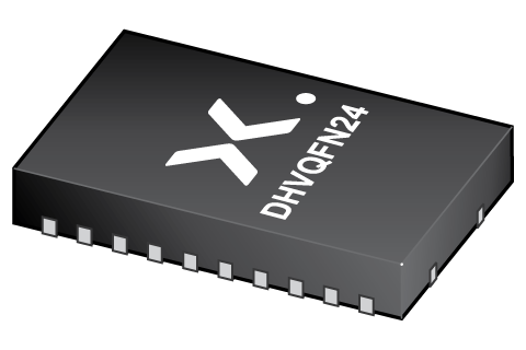
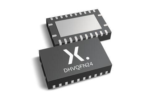
| 74LVC8T245BQ | 1.2 - 5.5 | 1.2 - 5.5 | CMOS/LVTTL | ± 24 | 3.5 | 8 | low | -40~125 | 66 | 5.8 | 40 | DHVQFN24 | Bi-directional | Direction controlled |
| 74LVC8T245BQ-Q100 | 1.2 - 5.5 | 1.2 - 5.5 | CMOS/LVTTL | ± 24 | 3.5 | 8 | low | -40~125 | 66 | 5.8 | 40 | DHVQFN24 | Bi-directional | Direction controlled |
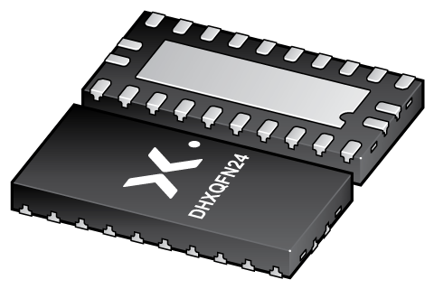
| 74LVC8T245BZ | 1.2 - 5.5 | 1.2 - 5.5 | CMOS/LVTTL | ± 24 | 3.5 | 8 | low | -40~125 | 111 | 72 | DHXQFN24 | Bi-directional | Direction controlled | |
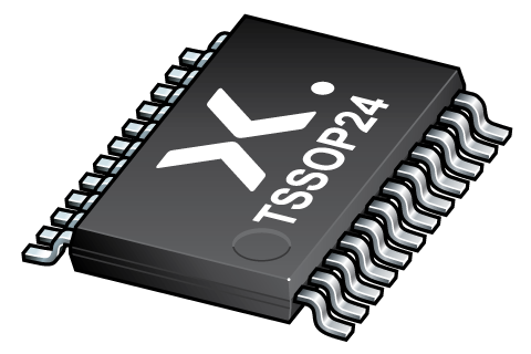
| 74LVC8T245PW | 1.2 - 5.5 | 1.2 - 5.5 | CMOS/LVTTL | ± 24 | 3.5 | 8 | low | -40~125 | 81 | 2.3 | 36 | TSSOP24 | Bi-directional | Direction controlled |
| 74LVC8T245PW-Q100 | 1.2 - 5.5 | 1.2 - 5.5 | CMOS/LVTTL | ± 24 | 3.5 | 8 | low | -40~125 | 81 | 2.3 | 36 | TSSOP24 | Bi-directional | Direction controlled |
| 74LVCH8T245BQ | 1.2 - 5.5 | 1.2 - 5.5 | CMOS/LVTTL | ± 24 | 3.5 | 8 | low | -40~125 | 66 | 5.8 | 40 | DHVQFN24 | Bi-directional | Direction controlled |
| 74LVCH8T245BQ-Q100 | 1.2 - 5.5 | 1.2 - 5.5 | CMOS/LVTTL | ± 24 | 3.5 | 8 | low | -40~125 | 66 | 5.8 | 40 | DHVQFN24 | Bi-directional | Direction controlled |
| 74LVCH8T245PW | 1.2 - 5.5 | 1.2 - 5.5 | CMOS/LVTTL | ± 24 | 3.5 | 8 | low | -40~125 | 81 | 2.3 | 36 | TSSOP24 | Bi-directional | Direction controlled |
| 74LVCH8T245PW-Q100 | 1.2 - 5.5 | 1.2 - 5.5 | CMOS/LVTTL | ± 24 | 3.5 | 8 | low | -40~125 | 81 | 2.3 | 36 | TSSOP24 | Bi-directional | Direction controlled |
Package
| Type number | Orderable part number, (Ordering code (12NC)) | Status | Marking | Package | Package information | Reflow-/Wave soldering | Packing |
|---|---|---|---|---|---|---|---|
| 74LVC8T245BQ | 74LVC8T245BQ,118 (935290138118) |
Active | LVC8T245 |
DHVQFN24 (SOT815-1) |
SOT815-1 | SOT815-1_118 | |
| 74LVC8T245BQ-Q100 | 74LVC8T245BQ-Q100J (935301104118) |
Active | LVC8T245 |
DHVQFN24 (SOT815-1) |
SOT815-1 | SOT815-1_118 | |
| 74LVC8T245BZ | 74LVC8T245BZX (935691146115) |
Active | YC8T245 |
DHXQFN24 (SOT8024-1) |
SOT8024-1 | SOT8024-1_115 | |
| 74LVC8T245PW | 74LVC8T245PW,118 (935290149118) |
Active | LVC8T245 |
TSSOP24 (SOT355-1) |
SOT355-1 |
SSOP-TSSOP-VSO-WAVE
|
SOT355-1_118 |
| 74LVC8T245PW-Q100 | 74LVC8T245PW-Q100J (935300465118) |
Active | LVC8T245 |
TSSOP24 (SOT355-1) |
SOT355-1 |
SSOP-TSSOP-VSO-WAVE
|
SOT355-1_118 |
| 74LVCH8T245BQ | 74LVCH8T245BQ,118 (935290148118) |
Active | VCH8T245 |
DHVQFN24 (SOT815-1) |
SOT815-1 | SOT815-1_118 | |
| 74LVCH8T245BQ-Q100 | 74LVCH8T245BQ-Q10J (935301103118) |
Active | VCH8T245 |
DHVQFN24 (SOT815-1) |
SOT815-1 | SOT815-1_118 | |
| 74LVCH8T245PW | 74LVCH8T245PW,118 (935290151118) |
Active | LVCH8T245 |
TSSOP24 (SOT355-1) |
SOT355-1 |
SSOP-TSSOP-VSO-WAVE
|
SOT355-1_118 |
| 74LVCH8T245PW-Q100 | 74LVCH8T245PW-Q10J (935301102118) |
Active | LVCH8T245 |
TSSOP24 (SOT355-1) |
SOT355-1 |
SSOP-TSSOP-VSO-WAVE
|
SOT355-1_118 |
Environmental information
| Type number | Orderable part number | Chemical content | RoHS | RHF-indicator |
|---|---|---|---|---|
| 74LVC8T245BQ | 74LVC8T245BQ,118 | 74LVC8T245BQ |
|
|
| 74LVC8T245BQ-Q100 | 74LVC8T245BQ-Q100J | 74LVC8T245BQ-Q100 |
|
|
| 74LVC8T245BZ | 74LVC8T245BZX | 74LVC8T245BZ |
|
|
| 74LVC8T245PW | 74LVC8T245PW,118 | 74LVC8T245PW |
|
|
| 74LVC8T245PW-Q100 | 74LVC8T245PW-Q100J | 74LVC8T245PW-Q100 |
|
|
| 74LVCH8T245BQ | 74LVCH8T245BQ,118 | 74LVCH8T245BQ |
|
|
| 74LVCH8T245BQ-Q100 | 74LVCH8T245BQ-Q10J | 74LVCH8T245BQ-Q100 |
|
|
| 74LVCH8T245PW | 74LVCH8T245PW,118 | 74LVCH8T245PW |
|
|
| 74LVCH8T245PW-Q100 | 74LVCH8T245PW-Q10J | 74LVCH8T245PW-Q100 |
|
|
Documentation (14)
| File name | Title | Type | Date |
|---|---|---|---|
| 74LVC_LVCH8T245 | 8-bit dual supply translating transceiver; 3-state | Data sheet | 2024-11-29 |
| AN90063 | Questions about package outline drawings | Application note | 2025-03-12 |
| Nexperia_document_guide_Logic_translators | Nexperia Logic Translators | Brochure | 2021-04-12 |
| SOT815-1 | 3D model for products with SOT815-1 package | Design support | 2019-10-03 |
| SOT8024-1 | 3D model for products with SOT8024-1 package | Design support | 2023-02-02 |
| SOT355-1 | 3D model for products with SOT355-1 package | Design support | 2020-01-22 |
| lvc8t245 | 74LVC8T245 IBIS model | IBIS model | 2021-02-02 |
| lvch8t245 | 74LVCH8T245 IBIS model | IBIS model | 2020-11-24 |
| Nexperia_package_poster | Nexperia package poster | Leaflet | 2020-05-15 |
| DHVQFN24_SOT815-1_mk | plastic, dual in-line compatible thermal enhanced very thin quad flat package; 24 terminals; 0.5 mm pitch; 3.5 mm x 5.5 mm x 0.85 mm body | Marcom graphics | 2017-01-28 |
| SOT815-1 | plastic, leadless dual in-line compatible thermal enhanced very thin quad flat package; 24 terminals; 0.5 mm pitch; 5.5 mm x 3.5 mm x 1 mm body | Package information | 2021-08-17 |
| SOT8024-1 | plastic, leadless dual in-line compatible thermal enhanced extreme thin quad flat package;no leads; 24 terminals; 0.4 mm pitch; body 2 mm x 4 mm x 0.48 mm | Package information | 2023-02-28 |
| SOT355-1 | plastic, thin shrink small outline package; 24 leads; 0.65 mm pitch; 7.8 mm x 4.4 mm x 1.2 mm body | Package information | 2024-11-15 |
| SSOP-TSSOP-VSO-WAVE | Footprint for wave soldering | Wave soldering | 2009-10-08 |
Support
If you are in need of design/technical support, let us know and fill in the answer form we'll get back to you shortly.
Models
| File name | Title | Type | Date |
|---|---|---|---|
| SOT815-1 | 3D model for products with SOT815-1 package | Design support | 2019-10-03 |
| SOT8024-1 | 3D model for products with SOT8024-1 package | Design support | 2023-02-02 |
| SOT355-1 | 3D model for products with SOT355-1 package | Design support | 2020-01-22 |
| lvc8t245 | 74LVC8T245 IBIS model | IBIS model | 2021-02-02 |
| lvch8t245 | 74LVCH8T245 IBIS model | IBIS model | 2020-11-24 |
Ordering, pricing & availability
Sample
As a Nexperia customer you can order samples via our sales organization.
If you do not have a direct account with Nexperia our network of global and regional distributors is available and equipped to support you with Nexperia samples. Check out the list of official distributors.