Package innovations
Continuously investing in new technologies
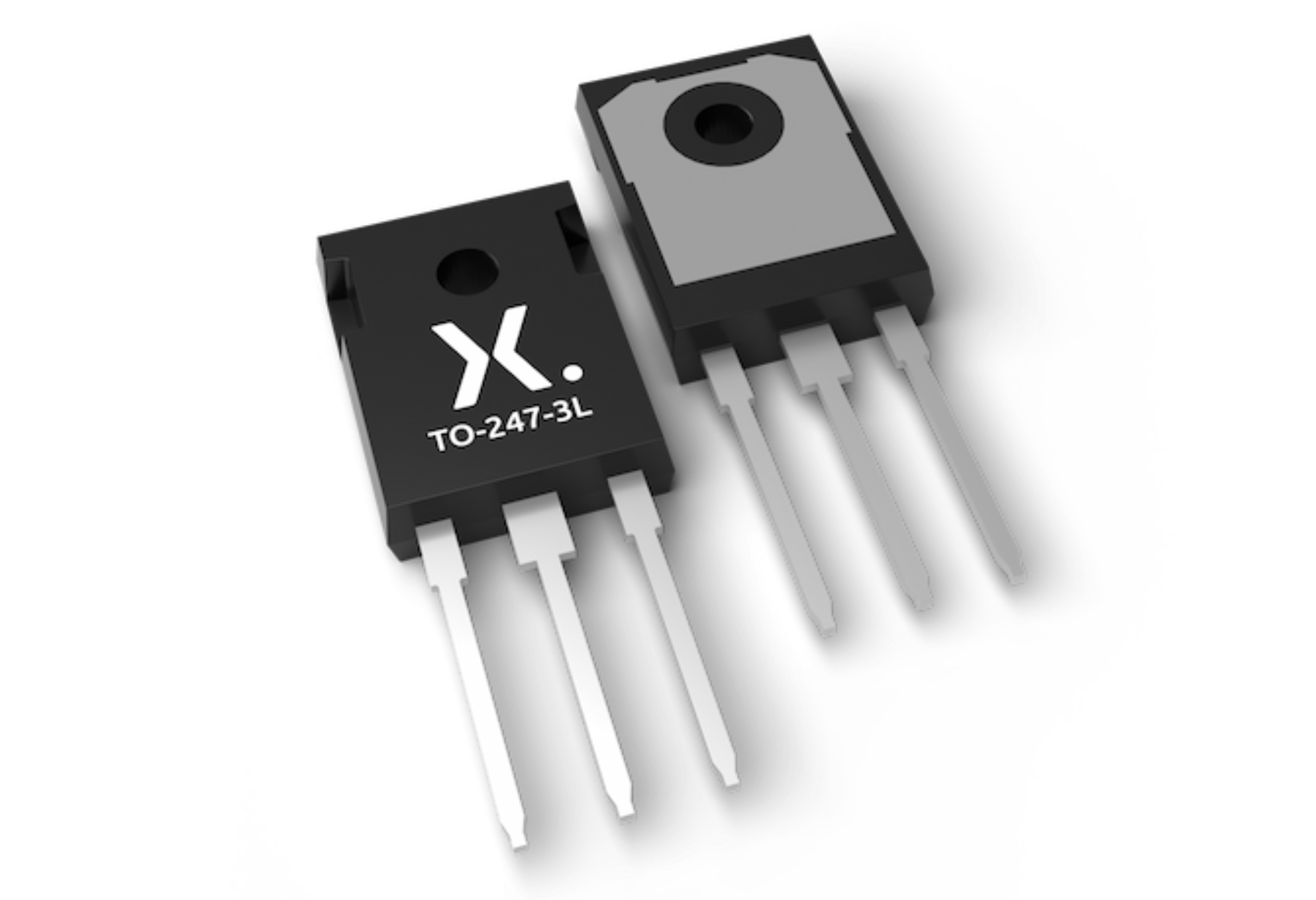
Integration and miniaturization have helped shrink electronic devices and revolutionize how we interact with the world around us. Of course this is not a new trend. In fact even before the introduction of the industry’s favourite SMD package (SOT23) in the 1960s, Nexperia has been pushing the boundaries of package technology to continuously deliver the right function in the right package with the right performance.
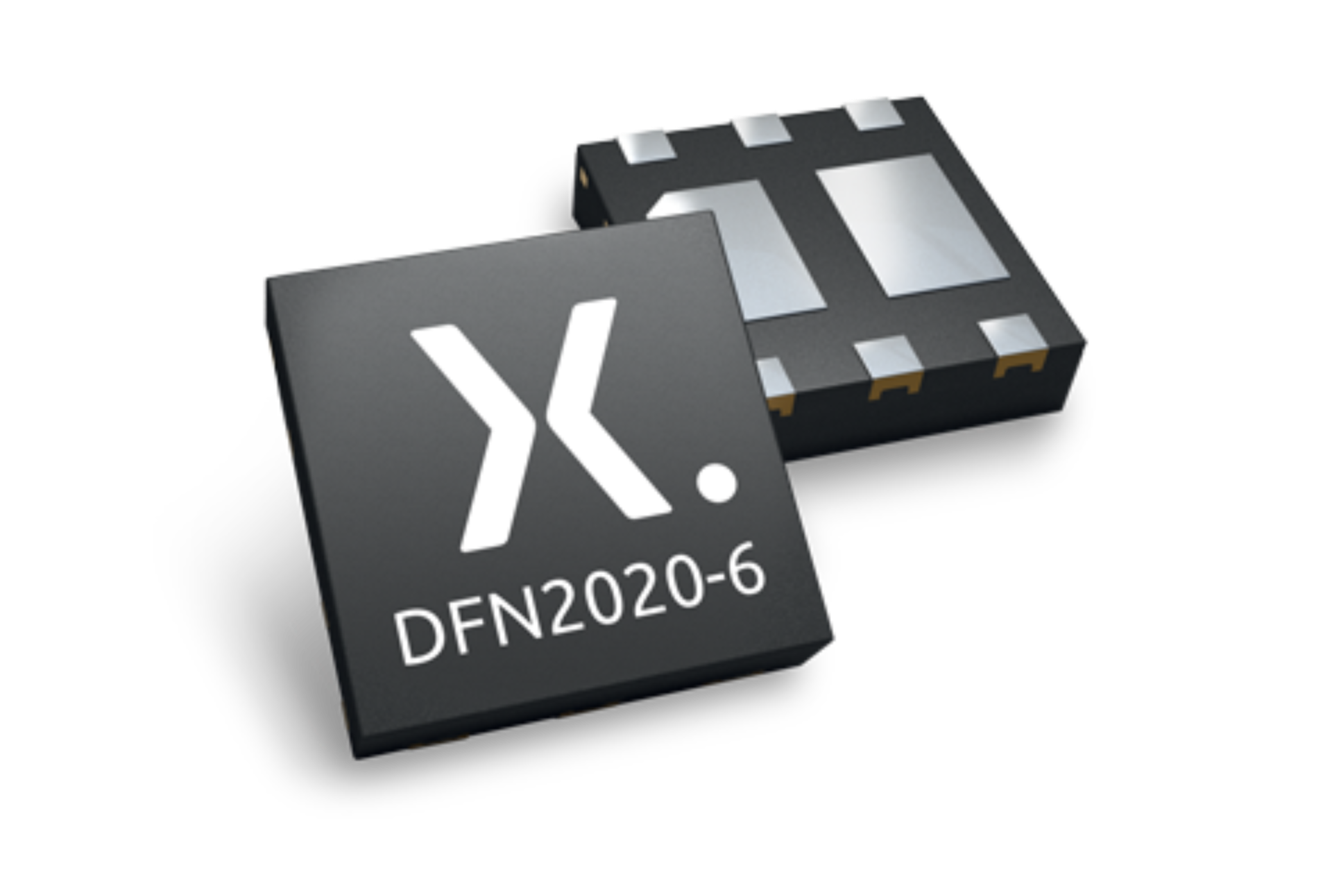
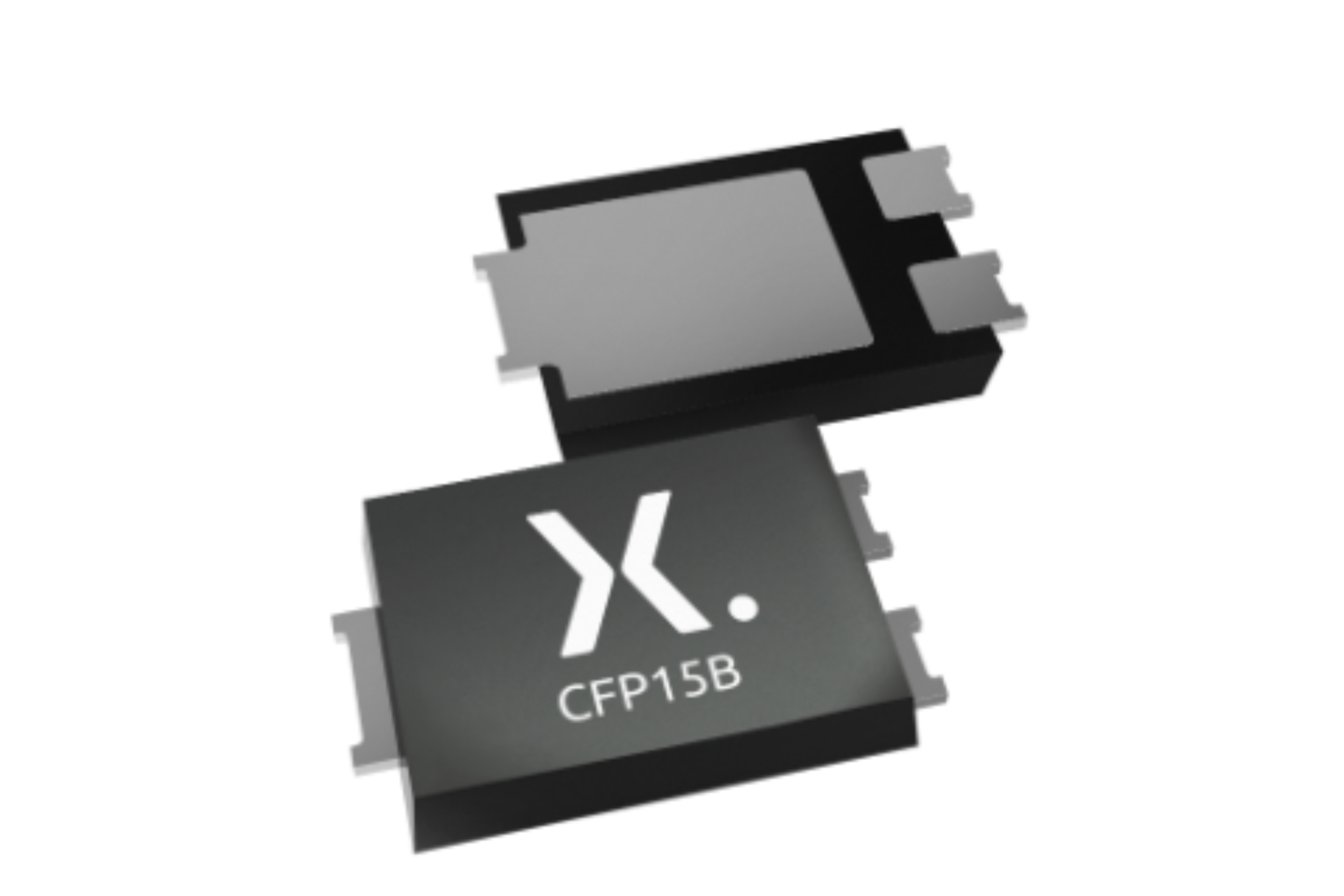
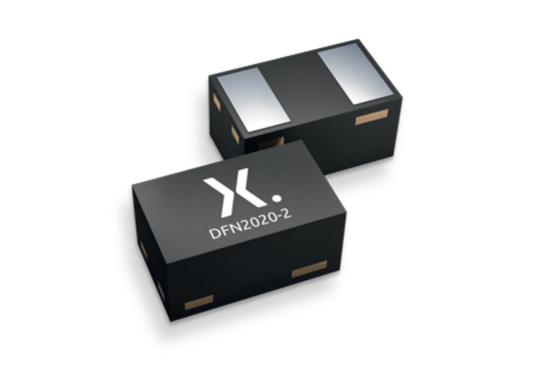
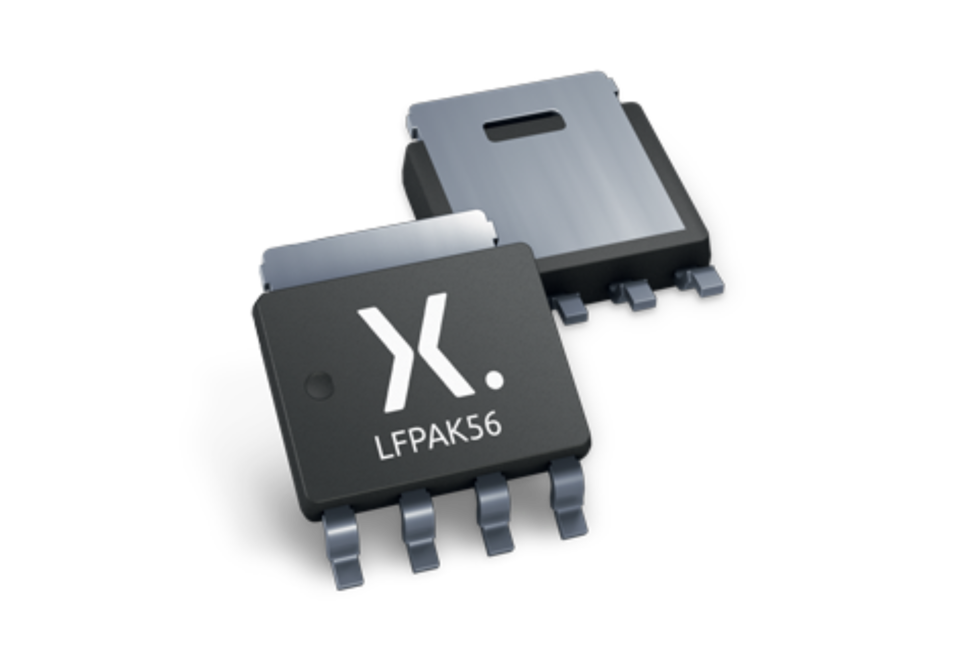
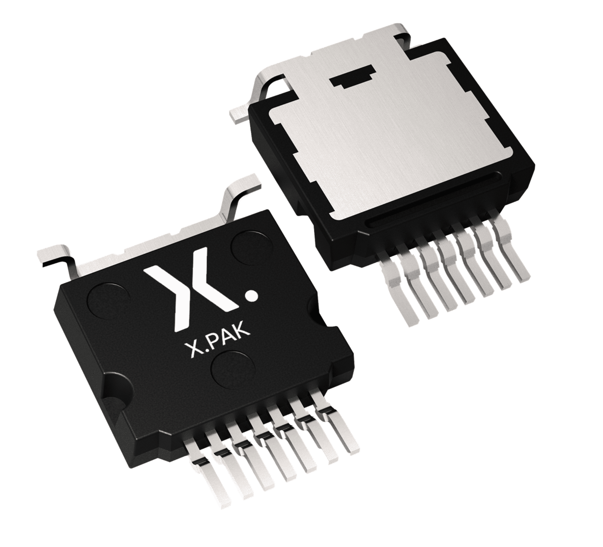
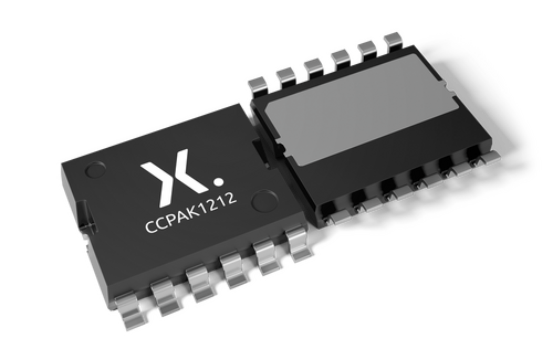
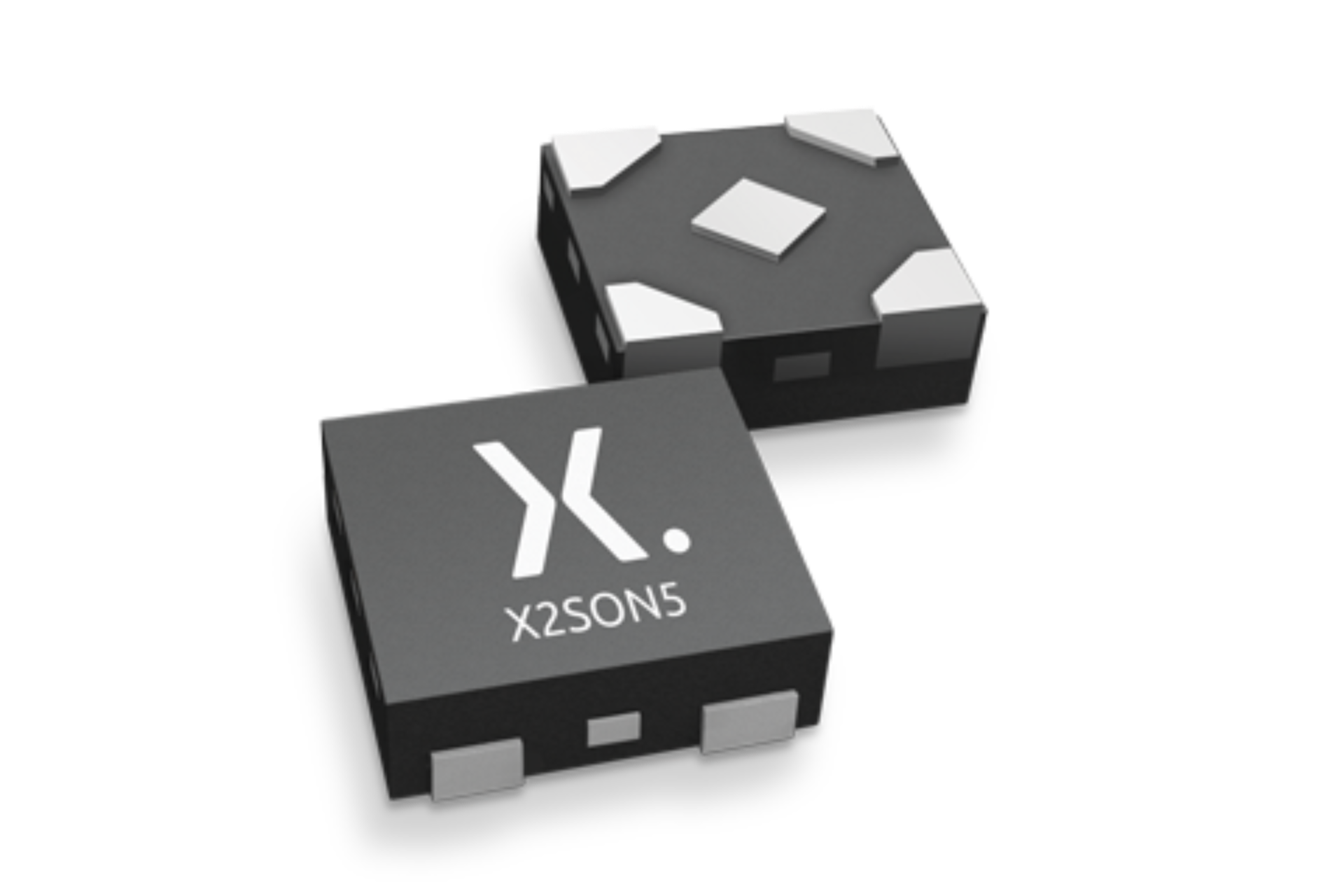
Today that focus in on efficiency. We continue to push towards ever more space efficient packages with chip-scale and near chip scale encapsulation options. From a performance perspective, our leaded clip-bond technology also delivers real thermal and package resistance benefits. And our leadless package options with side wettable flanks meet the demand for Automated Optical Inspection (AOI) of PCBs.
